Fabrication method of stamper for optical information recording medium, master disk of stamper for optical information recording medium, and optical information recording medium

a technology of optical information and recording medium, which is applied in the field of fabrication methods master disks of stampers for optical information recording medium, etc., can solve the problems of incorrect electroforming and inability to correctly perform electroforming

Inactive Publication Date: 2005-03-24
PANASONIC CORP
View PDF12 Cites 11 Cited by
  • Summary
  • Abstract
  • Description
  • Claims
  • Application Information

AI Technical Summary

Benefits of technology

[0071] The present invention makes it possible to provide a fabrication method of a stamper for an optical information recording medium by which electroforming can be preferably performed and a fine signal pit can be formed, a master disk of a stamper for an optical information recording medium, and an optical information recording medium.

Problems solved by technology

However, when fabricating a master disk in which a concave-convex signal pit of inorganic oxide resist is formed on a substrate and transferring and forming the concave-convex signal pit on the inorganic oxide resist to and on a metallic stamper through electroforming by the method disclosed in the document above, there is a problem that electroforming cannot be correctly performed.
In this case, cracks or exfoliation occurs in the chalcogen thin film 13, thereby the conductive film 16 is broken, and electroforming may not be correctly performed.

Method used


Image

  • Fabrication method of stamper for optical information recording medium, master disk of stamper for optical information recording medium, and optical information recording medium
  • Fabrication method of stamper for optical information recording medium, master disk of stamper for optical information recording medium, and optical information recording medium
  • Fabrication method of stamper for optical information recording medium, master disk of stamper for optical information recording medium, and optical information recording medium

Examples


embodiment 1

[0089] [Embodiment 1]

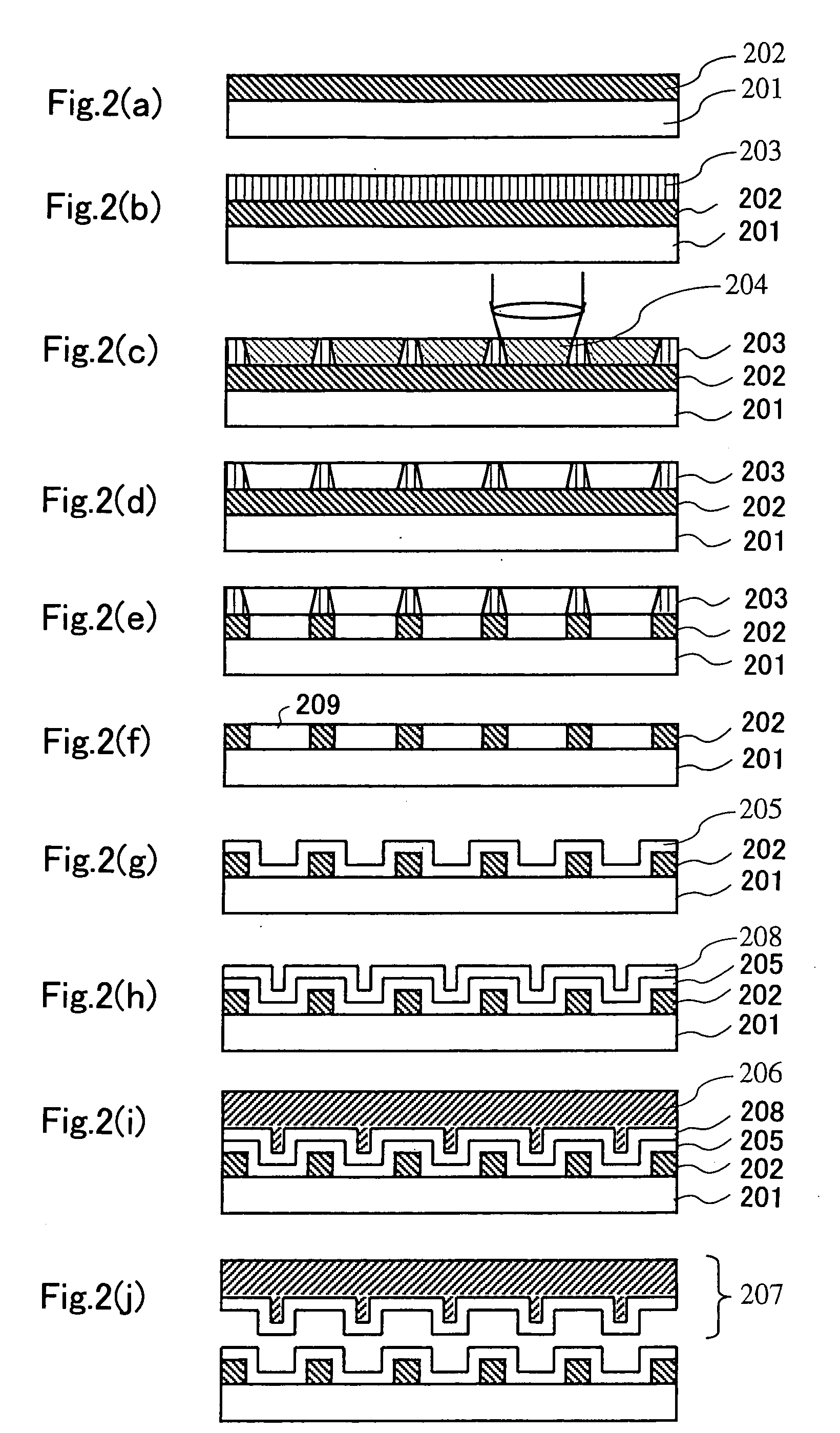
[0090] An example of the fabrication method of a stamper for an optical information recording medium of Embodiment 1 of the present invention is described below by referring to FIGS. 1(a) to 1(i). FIGS. 1(a) to 1(i) are illustrations showing steps of the fabrication method of a stamper for an optical information recording medium of the Embodiment 1.

[0091] First, an etching layer made of an acrylic material (content of 90% or more) 102 is formed on an Si substrate 101 through spin coating so that the thickness uniformly becomes approx. 60 nm over the entire surface (FIG. 1(a)).

[0092] Then, a resist layer 103 made of photoresist formed by an inorganic oxide material of TeOxPd (0102 (FIG. 1(b)).

[0093] Then, a laser beam whose intensity is modulated in accordance with a signal to be recorded and narrowed down by passing through a lens is applied through the surface of the resist layer 103 to change the crystal state of an exposed portion 104 (FIG. 1(c)).

[0094] T...

embodiment 2

[0128] [Embodiment 2]

[0129] Then, a fabrication method of a stamper for an optical information recording medium of Embodiment 2 of the present invention is described below by referring to FIG. 4. FIGS. 4(a) to 4(i) are illustrations showing steps of the fabrication method of a stamper for an optical information recording medium of the Embodiment 2 of the present invention.

[0130]FIG. 4 is different from FIG. 1 which shows the Embodiment 1 in material forming an etching layer. Though the etching layer 102 is formed by an acrylic material in FIG. 1, an etching layer 302 in FIG. 4 is formed by SiO2 (content of 90% or more). Other configuration in FIG. 4 is the same as that in FIG. 1.

[0131] First, the etching layer 302 of SiO2 is formed on an Si substrate 301 so that the thickness becomes almost uniform on the entire surface at approx. 60 nm (FIG. 4(a)).

[0132] Then, a resist layer 303 which is photoresist formed by an inorganic oxide material of TeOxPd (0302 (FIG. 4(b)).

[0133] Then, ...


PUM

PropertyMeasurementUnit
thicknessaaaaaaaaaa
thicknessaaaaaaaaaa
pit widthaaaaaaaaaa

Abstract

The following steps are included: a step of changing crystal states of the specific portion of an resist layer of a master disk having an etching layer and the resist layer formed on the etching layer through exposure, a step of removing the specific portion, a step of removing the portion of the etching layer overlapping the removed portion of the resist layer, a step of forming a conductive film from which the resist layer is removed, a step of performing electroforming by using the conductive film as an electrode, and a step of exfoliating the etching layer from the conductive film.

Description

BACKGROUND OF THE INVENTION [0001] 1. Field of the Invention [0002] The present invention relates to a fabrication method of a stamper for an optical information recording medium, a master disk of a stamper for an optical information recording medium, and an optical information recording medium in order to fabricate a high-density optical information recording medium in accordance with the dry etching method. [0003] 2. Related Art of the Invention [0004] Because an amount of information necessary for information apparatus and audiovisual apparatus increases, an optical disk superior in easiness for data access, accumulation of a large quantity of data and downsizing of apparatuses is noticed as an optical information recording medium and the density of information recorded thereof is increased. For example, a single-layer optical disk having a single-capacity of 25 GB is proposed in which the wavelength of a laser beam for reproducing a signal is set to approx. 400 nm as means of in...

Claims


Application Information

Patent Timeline
Patent Type & Authority Applications(United States)
IPC IPC(8): G11B7/24G11B7/26
CPCG11B7/24G11B7/263G11B7/261G11B7/26
Inventor TOMIYAMA, MORIOITO, EIICHIKAWAGUCHI, YUUKO
Owner PANASONIC CORP
Why Eureka
Try Eureka