
Method for forming a wiring of a semiconductor device, method for forming a metal layer of a semiconductor device and apparatus for performing the same

Inactive Publication Date: 2005-03-17
SAMSUNG ELECTRONICS CO LTD
View PDF10 Cites 123 Cited by
  • Summary
  • Abstract
  • Description
  • Claims
  • Application Information

AI Technical Summary

Benefits of technology

[0027] Embodiments of the present invention provide a method for forming a wiring of a semiconductor device, which is capable of performing a deposition process at a low temperature, readily embodying improved step coverage and having a simple processing parameter using a precursor that includes a tantalum amine derivative.
[0038] According to embodiments of the present invention, the metal wiring is formed using tantalum nitride as the precursor so that the metal wiring may have a rapid deposition speed and improved step coverage without defects. The metal wiring may be used as a metal barrier layer, a metal plug and so on.

Problems solved by technology

As a result, it has been more difficult to form a wiring.
However, since aluminum has a specific resistance of about 2.8×10⁸ Ωm and tungsten has a specific resistance of about 5.5×10⁸ Ωm, aluminum and tungsten are inappropriate for the metal wiring of the multi-layered structure.
As a result, the titanium nitride layer is not well suited as a metal barrier layer.
As a result, a ring defect may be generated along the interface between grains of aluminum.
The ring defect induces a short between metal wirings, thereby deteriorating characteristic and reliability of a semiconductor device.
Furthermore, since the interval between the metal wirings is reduced due to the high integration of a semiconductor device, the ring effect is a greater problem.
However, this solution complicates the formation of the metal wiring, as will be explained further.
However, when the conductive layer pattern is exposed through the via hole, the reliability of the lower wiring may be reduced.
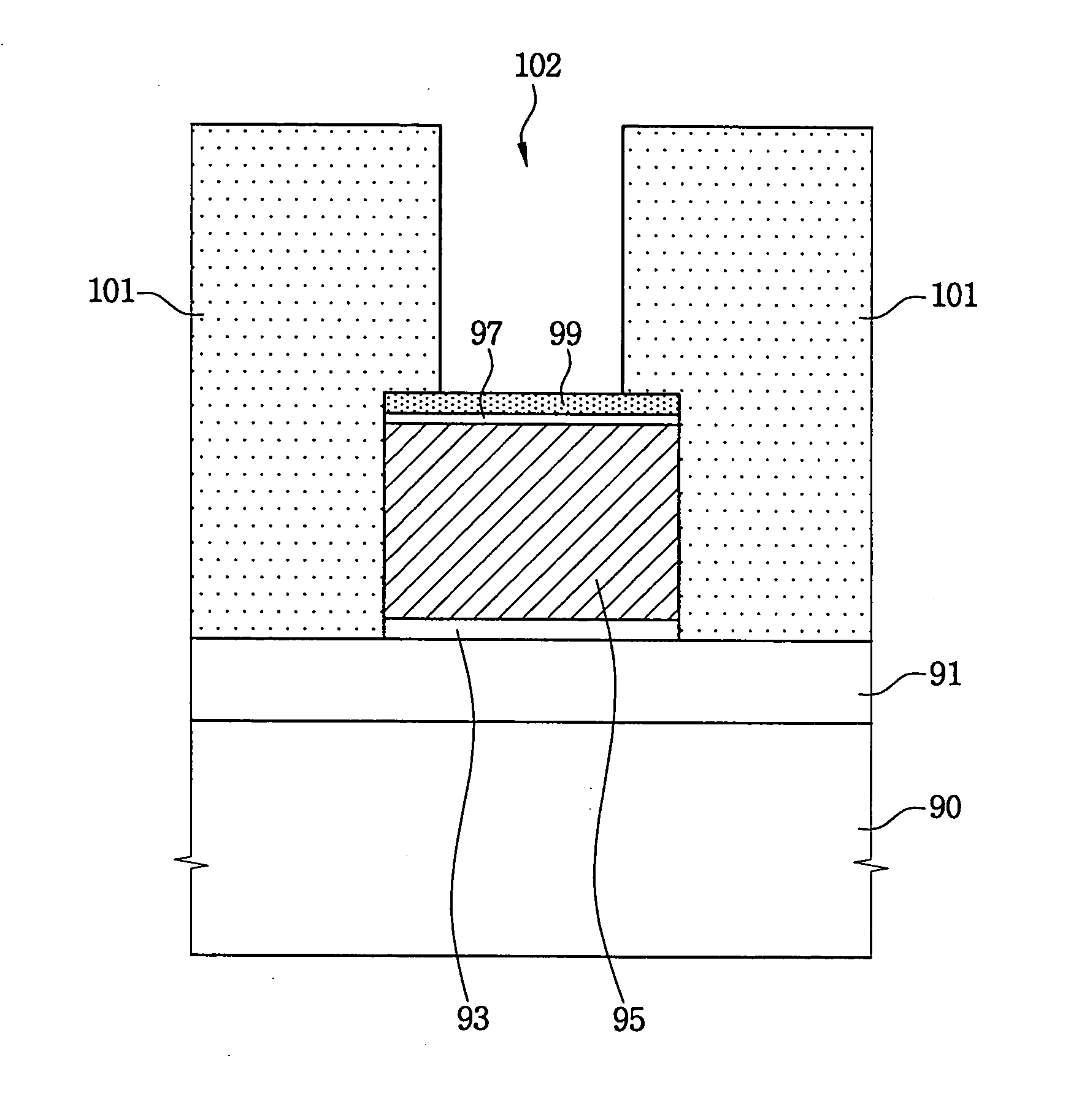
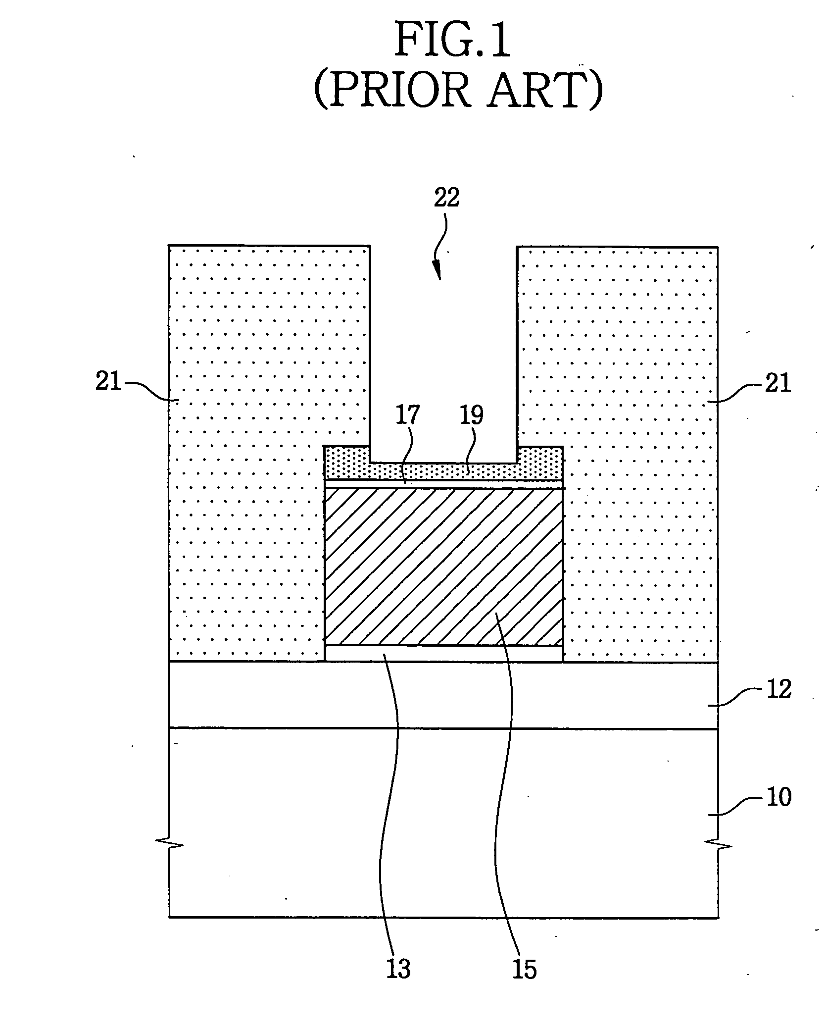
However, when the reflection preventing layer 19 has a sufficient thickness, filling the space between the wirings with the insulating interlayer 21 may be difficult and may create the aforementioned void.
Since the process is performed at a high temperature, a thermal attack may be applied to a semiconductor device making the CVD process more difficult.
Since the power source is directly applied to a substrate, the substrate may be damaged.
Particularly, when the MOCVD process is performed on the substrate using only Ta(NC(Ch3)2C2HS)(N(CH3)2)3), the pressure in the chamber is not sufficiently high and the MOCVD process may be ineffective.

Method used


Image

  • Method for forming a wiring of a semiconductor device, method for forming a metal layer of a semiconductor device and apparatus for performing the same
  • Method for forming a wiring of a semiconductor device, method for forming a metal layer of a semiconductor device and apparatus for performing the same
  • Method for forming a wiring of a semiconductor device, method for forming a metal layer of a semiconductor device and apparatus for performing the same

Examples


example 1

[0150] A via resistance of a semiconductor device having a Kelvin structure that included a single via formed between lower and upper wirings was shown in FIG. 10.

[0151] A tantalum nitride layer having a thickness of about 300 Å was formed on a substrate by a conventional PVD process. On the contrary, a first tantalum nitride layer having a thickness of about 5 Å was formed on a substrate by an ALD process in accordance with the method of the present invention. A second tantalum nitride layer having a thickness of about 10 Å was formed on a substrate by an ALD process in accordance with the method of the present invention. A third tantalum nitride layer having a thickness of about 15 Å was formed on a substrate by an ALD process in accordance with the method of the present invention. The four substrates had via holes having a diameter of about 0.13 μm, respectively.

[0152] As shown in FIG. 10, the tantalum nitride layers formed by the method of the present invention had thickness t...

example 2

[0153] A characteristic of leakage currents in a semiconductor device having a single damascene comb structure that included a trench filled with wirings was shown in FIG. 11. The wirings had a length of about 3.6 meters, a width of about 0.141 μm and an interval therebetween of about 0.14 mm. In FIG. 11, a lateral axis represented a leakage current and a longitudinal axis represented a cumulative probability.

[0154] A tantalum nitride layer having a thickness of about 300 Å was formed on a substrate by a conventional PVD process, whereas, a tantalum nitride layer having a thickness of about 10 Å was formed on a substrate by an ALD process in accordance with the method of the present invention. In FIG. 11, line a indicates the characteristic of leakage current of the tantalum nitride layer formed by the conventional method. Line b indicates the characteristic of leakage current of the tantalum nitride layer formed by the method of the present invention. As shown in FIG. 11, it could...

example 3

[0155] A via resistance of tantalum nitride barrier layers was shown in FIG. 12. A via plug had a critical dimension of about 0.26 mm and an aspect ratio of about 3.1:1. In FIG. 12, [a]line a indicates a via resistance of a tantalum nitride layer when ((Net2)3Ta=NtBu) was used as a precursor. Line b indicates a via resistance of a tantalum nitride layer when Ta(NC(Ch3)2C2H5)(N(CH3)2)3) was used as a precursor. Aluminum layers were formed on the tantalum nitride barrier layers, respectively.

[0156] As shown in FIG. 12, the via resistance was directly proportional to a thickness of the tantalum nitride barrier layer. It could be noted that the tantalum nitride barrier layer formed using Ta(NC(Ch3)2C2H5)(N(CH3)2)3) as the precursor had a via resistance lower than that formed using ((Net2)3Ta═NtBu) as the precursor.


PUM

PropertyMeasurementUnit
Temperatureaaaaaaaaaa

Abstract

In a method for forming a wiring of a semiconductor device using an atomic layer deposition, an insulating interlayer is formed on a substrate. Tantalum amine derivatives represented by a chemical formula Ta(NR1)(NR2R3)3 in which R1, R2 and R3 represent H or C1-C6 alkyl group are introduced onto the insulating interlayer. A portion of the tantalum amine derivatives is chemisorbed on the insulating interlayer. The rest of tantalum amine derivatives non-chemisorbed on the insulating interlayer is removed from the insulating interlayer. A reacting gas is introduced onto the insulating interlayer. A ligand in the tantalum amine derivatives chemisorbed on the insulating interlayer is removed from the tantalum amine derivatives by a chemical reaction between the reacting gas and the ligand to form a solid material including tantalum nitride. The solid material is accumulated on the insulating interlayer through repeating the above processes to form a wiring.

Description

CROSS REFERENCE TO RELATED APPLICATION [0001] This application is a Continuation-In-Part of U.S. patent application Ser. No. 10 / 196,814, entitled “METHODS OF FORMING METAL LAYERS USING METALLIC PRECURSORS”, filed on Jul. 17, 2002, of U.S. patent application Ser. No. 10 / 461,613, entitled “SEMICONDUCTOR INTERCONNECTION STRUCTURE WITH TaN AND METHOD OF FORMING THE SAME”, filed on Jun. 13, 2003, and of U.S. patent application Ser. No. 10 / 404,360, entitled “METHOD AND APPARATUS FOR FORMING A METAL LAYER ON A SEMICONDUCTOR DEVICE,” filed on Apr. 1, 2003. This application also claims priority from Korean Patent Application No. 2003-33905, filed on May 28, 2003, the contents of which are herein incorporated by reference in their entirety for all purposes.BACKGROUND OF THE INVENTION [0002] 1. Field of the Invention [0003] This disclosure relates to semiconductor devices. More particularly, this disclosure relates to a method for forming a wiring[of a semiconductor device, for example, such a...

Claims


Application Information

Patent Timeline
IPC IPC(8): H01L21/00H01L21/44H01L21/84
CPCC23C16/34C23C16/45553H01L21/28556H01L21/28562H01L21/76877H01L21/7685H01L21/76858H01L21/76862H01L21/76867H01L21/76843
Inventor CHOI, KYUNG-INKANG, SANG-BOMPARK, SEONG-GEONLEE, YOU-KYOUNGCHOI, GIL-HEYUNLEE, JONG-MYEONGLEE, SANG-WOO
Owner SAMSUNG ELECTRONICS CO LTD
Learn More