Electro-optical device and manufacturing method thereof

a manufacturing method and optical technology, applied in the direction of discharge tube/lamp details, discharge tube luminescnet screens, gas-filled discharge tubes, etc., can solve the problems of enormous processing time of this method for forming the el layers corresponding to each pixel electrode, and achieve high thermal conductivity, prevent the transmission of alkali metals, and high heat radiating

Inactive Publication Date: 2005-02-17
SEMICON ENERGY LAB CO LTD
View PDF99 Cites 111 Cited by
  • Summary
  • Abstract
  • Description
  • Claims
  • Application Information

AI Technical Summary

Benefits of technology

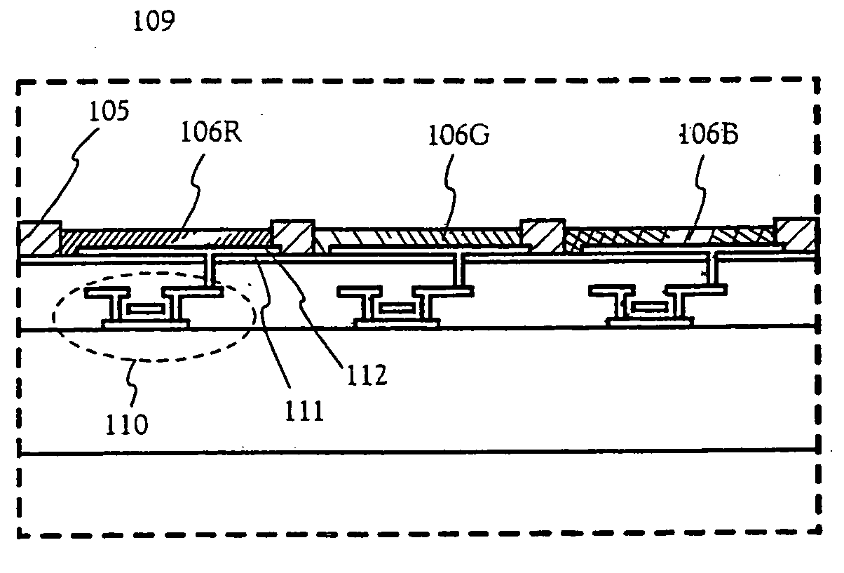
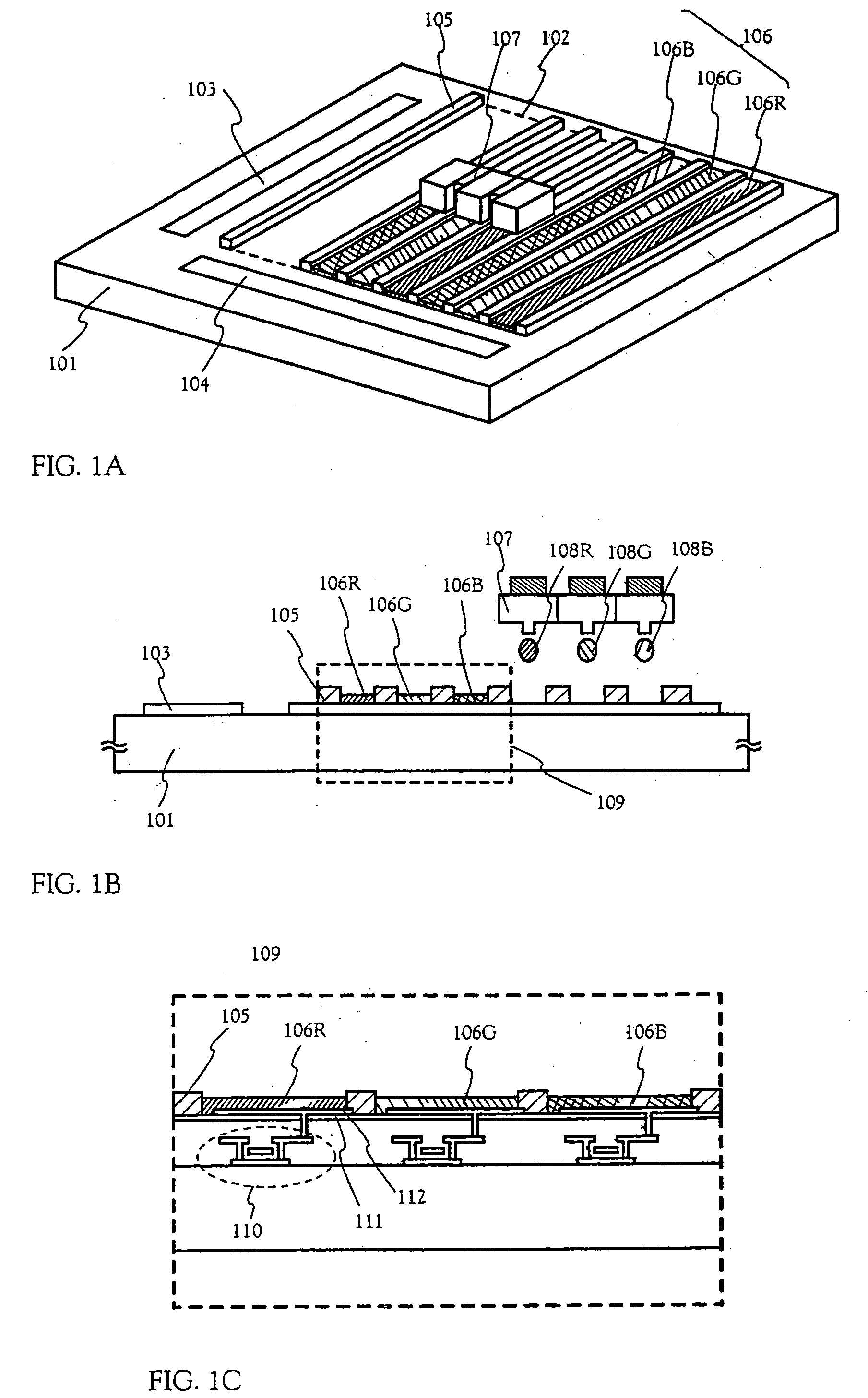
[0010] The present invention aims to simplify the formation of an EL layer by an ink-jet method, and to perform high speed processing. An object of the present invention is to provide a method of manufacturing a high operation performance, high reliability electro-optical device, in particular a method of manufacturing an EL display device. In addition, an object of the present invention is to increase the quality of an electronic device having the EL display device as a display by increasing the picture quality of the electro-optical device.
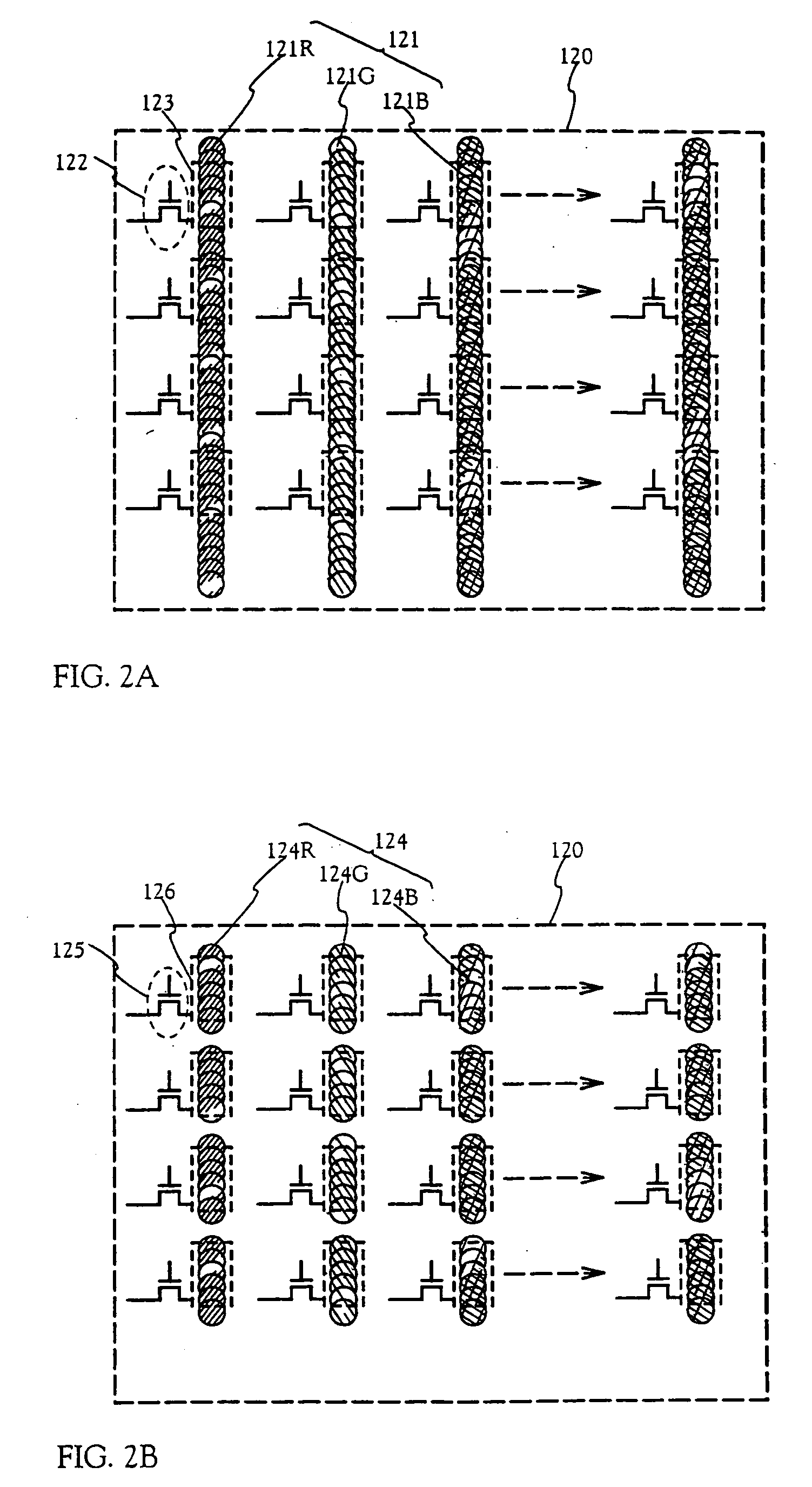
[0012] A predetermined pattern is formed with the ink jet method by repeatedly performing positional control of an ink head and discharge of ink (when an EL layer is formed, a liquid containing the EL layer material). Note that if the screen size becomes large or the pixel density becomes high, then the amount of processing time by this method for forming the EL layers corresponding to each pixel electrode becomes enormous. However, with the above method of forming the stripe state or the oblong or rectangular shapes, it becomes possible to form the EL layers by continuously scanning the ink head and the amount of processing time can be shortened.
[0014] In addition, the diffusion of alkali metals from EL elements formed by the ink-jet method is prevented by an insulating film (passivation film) formed between the EL elements and TFTs with the present invention. Specifically, an insulating film for preventing transmission of alkali metals is formed on a leveling film covering the TFTs. In other words, a material may be used in which the diffusion speed of alkali metals throughout the insulating film at the operation temperature of the EL display device is sufficiently low.

Problems solved by technology

Note that if the screen size becomes large or the pixel density becomes high, then the amount of processing time by this method for forming the EL layers corresponding to each pixel electrode becomes enormous.

Method used


Image

  • Electro-optical device and manufacturing method thereof
  • Electro-optical device and manufacturing method thereof
  • Electro-optical device and manufacturing method thereof

Examples


embodiment 1

[0122] [Embodiment 1]

[0123] The embodiments of the present invention are explained using FIGS. 7A to 9C. A method of simultaneous manufacture of a pixel portion, and TFTs of a driver circuit portion formed in the periphery of the pixel portion, is explained here. Note that in order to simplify the explanation, a CMOS circuit is shown as a basic circuit for the driver circuits.

[0124] First, as shown in FIG. 7A, a base film 301 is formed with a 300 nrm thickness on a glass substrate 300. Silicon nitride oxide films are laminated as the base film 302 in embodiment 1. It is good to set the nitrogen concentration at between 10 and 25 wt % in the film contacting the glass substrate 300.

[0125] Besides, as a part of the base film 301, it is effective to provide an insulating film made of a material similar to the first passivation film 41 shown in FIG. 5. The current controlling TFT is apt to generate heat since a large current is made to flow, and it is effective to provide an insulating...

embodiment 2

[0199] [Embodiment 2]

[0200] An EL display device having a form in which light emitted by an EL element is irradiated to the side of a substrate on which TFTs are formed is shown in Embodiment 1. For this case, at least the region in which the TFTs are formed becomes shadow, and the aperture ratio of a pixel portion is reduced by that amount. On the other hand, if a form is used in which light emitted by the EL element is irradiated in the upward direction (the side of the substrate opposite that on which the TFTs are formed), then at least it becomes easy to increase the aperture ratio.

[0201]FIG. 18 shows the structure of an EL display element in which tight is irradiated in the upward direction. The structures of the switching TFT 201 and the current control TFT 202 are the same as those of Embodiment Mode 2, and the differences in other portions is explained here.

[0202] A cathode side pixel electrode 949 connected to the drain side of the current control TFT 202 is formed on a s...

embodiment 3

[0204] [Embodiment 3]

[0205] The method of manufacturing an EL layer by an ink-jet method, and the manufactured EL layer according to the present invention, can also be applied to a passive type EL display device. An example of such is explained with reference to FIGS. 16A to 16E.

[0206] A substrate such as: a non-alkaline glass substrate, typically a Coming Corp. # 1737 glass substrate; a crystalline glass substrate; a soda lime glass substrate on whose surface a silicon oxide film or a silicon nitride film is formed; or a plastic substrate can be applied to a substrate 1601 in FIG. 16A. A transparent electrode 1602 is formed with a film thickness of 50 to 200 μm on the substrate 1601, and is partitioned into a plurality of strip shapes by a process such as etching or lift-off. The transparent electrode 1601 is formed from a material such as ITO, ZnO, SnO2, or ITO-ZnO. Then, using an organic resin material such as polyimide, separating layers 1603 are formed with a thickness of 0.5 ...


PUM


Abstract

The present invention aims to provide simple, high-speed processing for the formation of an EL layer by an ink-jet method. A method of manufacturing an electro-optical device having good operation performance and high reliability, and in particular, a method of manufacturing an EL display device, is provided. The present invention forms EL layers continuously across a plurality of pixels when the EL layers are formed by the ink-jet method. Specifically, with respect to m columns and n rows of pixel electrodes arranged in a matrix state, the EL layers are formed so as to form stripes with respect to one certain selected row or one column. The EL layers may also be formed having an oblong shape or a rectangular shape with respect to each pixel electrode.

Description

BACKGROUND OF THE INVENTION [0001] 1. Field of the Invention [0002] The present invention relates to an electro-optical device typified by an EL (electroluminescence) display device formed by fabricating semiconductor elements (elements using a semiconductor thin film) on a surface of a substrate, and an electronic device including the electro-optical device as a display. Particularly, the invention relates to a method of manufacturing the same. [0003] 2. Description of the Related Art [0004] In recent years, a technique for forming a thin film transistor (hereinafter referred to as a “TFT”) on a substrate has made remarkable progress, and its application and development to an active matrix type display device has proceeded. Especially, since a TFT using a semiconductor film that has a crystal structure (e.g., a polysilicon film) has a field effect mobility higher than a conventional TFT using an amorphous silicon film, a high speed operation can be made. Thus, it becomes possible t...

Claims


Application Information

Patent Timeline
Patent Type & Authority Applications(United States)
IPC IPC(8): H01L21/77H01L21/84H01L31/12H01L27/12H01L27/32H01L51/00H01L51/40H01L51/52H05B33/10H05B44/00
CPCH01L27/12H01L27/1214H01L27/3211H01L27/3244H01L51/524H01L27/3258H01L51/0005H01L51/5228H01L27/3246H01L29/78621H01L29/78624H01L29/78627H01L29/78645H10K59/35H10K59/124H10K59/122H10K59/12H10K71/135H10K50/824H10K50/841H01L31/12H05B33/10
Inventor YAMAZAKI, SHUNPEIYAMAMOTO, KUNITAKAARAI, YASUYUKI
Owner SEMICON ENERGY LAB CO LTD
Why Eureka
Try Eureka