
Organic light-emitting display device and method of manufacturing the same

a technology of organic light-emitting display and display device, which is applied in the direction of solid-state devices, semiconductor devices, thermoelectric devices, etc., can solve the problems of difficult use of fine metal masks that are often used in conventional patterning processes, and achieve the effect of reducing the wiring resistance of the common electrode and simplifying the formation of opening patterns

Active Publication Date: 2015-03-31
SAMSUNG DISPLAY CO LTD
View PDF15 Cites 31 Cited by
  • Summary
  • Abstract
  • Description
  • Claims
  • Application Information

AI Technical Summary

Benefits of technology

[0007]Embodiments of the present invention provide for an organic light-emitting display device having simplified formation of an opening pattern of a common electrode, and decreased wiring resistance of the common electrode. Further embodiments of the present invention provide for a method of manufacturing such an organic light-emitting display device.

Problems solved by technology

However, forming an opening pattern in a cathode, which may be a common electrode, makes it difficult to use a fine metal mask that is often used in a conventional patterning process.

Method used


Image

  • Organic light-emitting display device and method of manufacturing the same
  • Organic light-emitting display device and method of manufacturing the same
  • Organic light-emitting display device and method of manufacturing the same

Examples


Embodiment Construction

[0054]Now, exemplary embodiments according to the present invention will be described in detail with reference to the accompanying drawings. As used herein, the term “and / or” includes any and all combinations of one or more of the associated listed items. Expressions such as “at least one of,” when preceding a list of elements, modify the entire list of elements and do not modify the individual elements of the list.

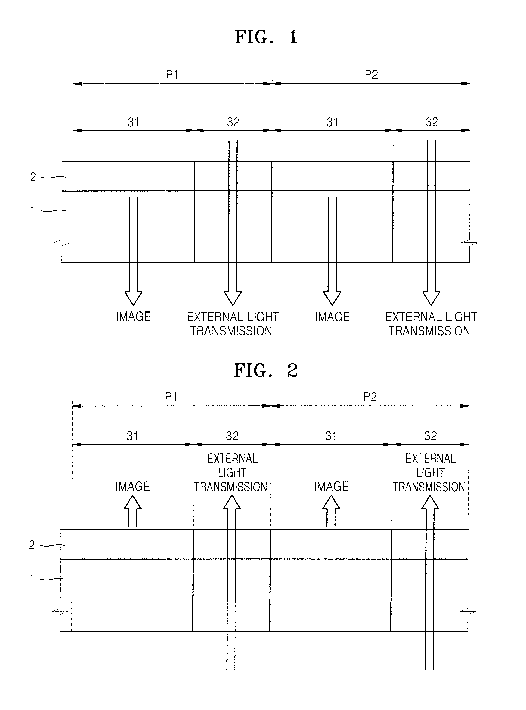
[0055]FIG. 1 is a schematic cross-sectional view of an organic light-emitting display device according to an embodiment of the present invention.

[0056]Referring to FIG. 1, the organic light-emitting display device includes a substrate 1 and a display unit 2 formed on the substrate 1. In the organic light-emitting display device, external light penetrates the substrate 1 and the display unit 2. For example, external light enters one side of the organic light-emitting display device, transmits through the display unit 2 and the substrate 1, and exits another side of the org...


PUM


Abstract

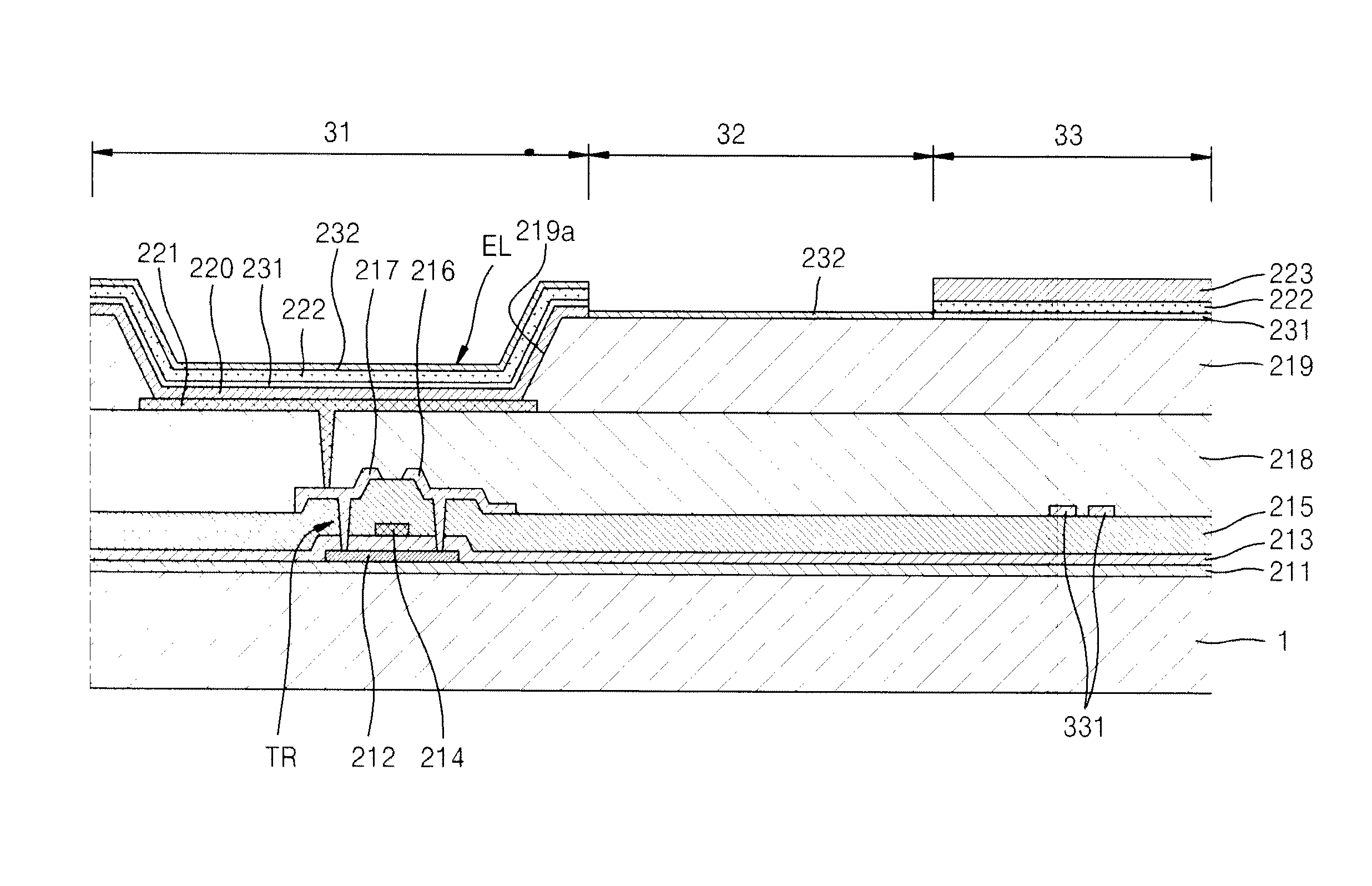
An organic light-emitting display device and a method of manufacturing the organic light-emitting display device are provided. The organic light-emitting display device includes a plurality of pixels each including: a first region including a light-emitting region for emitting light, a first electrode and an emission layer covering the first electrode being located in the light-emitting region; and a second region including a transmissive region for transmitting external light through the display device. The display device also includes: a third region between the pixels; a first auxiliary layer in the first and third regions; a second electrode on the first auxiliary layer in the first and third regions; a second auxiliary layer covering the second electrode and located in the first and second regions and not in the third region; and a third electrode on the second electrode in the third region.

Description

CROSS-REFERENCE TO RELATED PATENT APPLICATION[0001]This application claims priority to and the benefit of Korean Patent Application No. 10-2012-0062347, filed on Jun. 11, 2012 in the Korean Intellectual Property Office, the entire content of which is incorporated herein by reference.BACKGROUND[0002]1. Field[0003]Aspects of embodiments of the present invention relate to an organic light-emitting display device and a method of manufacturing the organic light-emitting display device.[0004]2. Description of the Related Art[0005]Organic light-emitting display devices are self-emitting display devices that electrically excite organic compounds to emit light. Organic light-emitting display devices have drawn attention as next-generation display devices capable of resolving problems that have been pointed out in liquid crystal display devices because organic light-emitting display devices may be driven at lower voltages, may be more easily made thin, may have wider viewing angles, and may h...

Claims


Application Information

Patent Timeline
Patent Type & Authority Patents(United States)
IPC IPC(8): H01L29/08H01L51/00H01L21/00H01L27/32H01L51/50H01L51/56
CPCH01L51/5008H01L51/56H01L27/3244H10K59/12H10K59/121H10K59/1315H10K71/20H10K71/60H10K71/621H10K50/814H10K50/85H10K71/80H10K59/1201H10K71/00H10K2102/3031H10K30/865H10K2102/351H10K50/81H10K50/828
Inventor CHOI, JUN-HOCHUNG, JIN-KOOKIM, SEONG-MIN
Owner SAMSUNG DISPLAY CO LTD
Learn More