Multiple oxidation smoothing method for reducing silicon waveguide roughness

a silicon waveguide and multi-oxidation technology, applied in the field of optical communication, can solve the problems of detriment to choosing this smoothing technique, low roughness of waveguides, and substantial roughness on the sidewalls, so as to reduce the overall time of oxidation and volume of oxidized materials, reduce the roughness of sidewalls, and reduce the roughness of waveguides

Active Publication Date: 2005-01-20
MASSACHUSETTS INST OF TECH
View PDF3 Cites 4 Cited by
  • Summary
  • Abstract
  • Description
  • Claims
  • Application Information

AI Technical Summary

Benefits of technology

[0007] According to one aspect of the invention, there is provided a method of reducing waveguide roughness. The method includes oxidizing the surface of a waveguide to form an oxidized layer. The method also includes isotropically etching the oxidized layer every time a reaction-limited regime is approaching a diffusion-limited regime. The oxidized layer is repeatedly oxidized and etched so that a waveguide is continuously oxidized in the reaction-limited regime, reducing the overall time of oxidation and volume of oxidized material so that the waveguide has its sidewall roughness reduced efficiently enabling high transmission rates of guided light.
[0008] According to another aspect of the invention, there is provided a light-guiding structure. The light-guiding structure includes a waveguide structure that comprises a substrate and a low refractive index underclad material. The waveguide structure is oxidized to form an oxidized layer on a surface of the waveguide structure. The oxidized layer is isotropically etched after the reaction-limited oxidation regime is approaching the diffusion-limited regime and repeatedly oxidized and etched so that the waveguide structure is continuously oxidized in the reaction-limited regime, reducing the overall time of oxidation and volume of oxidized material so that the waveguide structure has its sidewall roughness reduced efficiently enabling high transmission rates of guided light.
[0009] According to one aspect of the invention, there is provided a method of reducing waveguide roughness. The method includes forming a compound layer on a surface of a waveguide by exposure to a reactive ambient. The method also includes removing the compound layer every time a reaction-limited regime is approaching a diffusion-limited regime. The compound layer is repeatedly exposed and removed so that a waveguide is continuously exposed in the reaction-limited regime, reducing the overall time of exposure and volume of the compound layer materials so that the waveguide has its sidewall roughness reduced efficiently enabling high transmission rates of guided light.
[0010] According to another aspect of the invention, there is provided a light-guiding structure. The light-guiding structure includes a light-guiding structure comprising a waveguide structure that comprises a substrate and a low refractive index underclad material The waveguide structure is exposed to a reactive ambient to form an compound layer on a surface of said waveguide structure. The compound layer is removed after the reaction-limited regime is approaching the diffusion-limited regime and repeatedly exposed and removed so that the waveguide structure is continuously exposed in the reaction-limited regime, reducing the overall time of exposure and volume of the compound layer material so that said waveguide structure has its sidewall roughness reduced efficiently enabling high transmission rates of guided light.

Problems solved by technology

This typically leaves waveguides with minimal roughness on the top and bottom of the waveguide but substantial roughness on the sidewalls.
There are several detriments to choosing this smoothing technique.
If the waveguide is polycrystalline, the effect of an anisotropic etch is unpredictable.
Not all aspects of anisotropic etching are detrimental though.
There are several detriments with this method as well.
First, typical silicon waveguide roughness requires several hours of high temperature oxidation to smooth the roughness to a level that allows for sufficient light transmission.
This is dire for chip. designers who have tight thermal budgets and do not want diffusion to occur in other parts of the chip.
However, significant material is removed, and critical dimensional control is lost.
The two methods described above have undesirable detriments.

Method used


Image

  • Multiple oxidation smoothing method for reducing silicon waveguide roughness
  • Multiple oxidation smoothing method for reducing silicon waveguide roughness
  • Multiple oxidation smoothing method for reducing silicon waveguide roughness

Examples


Embodiment Construction

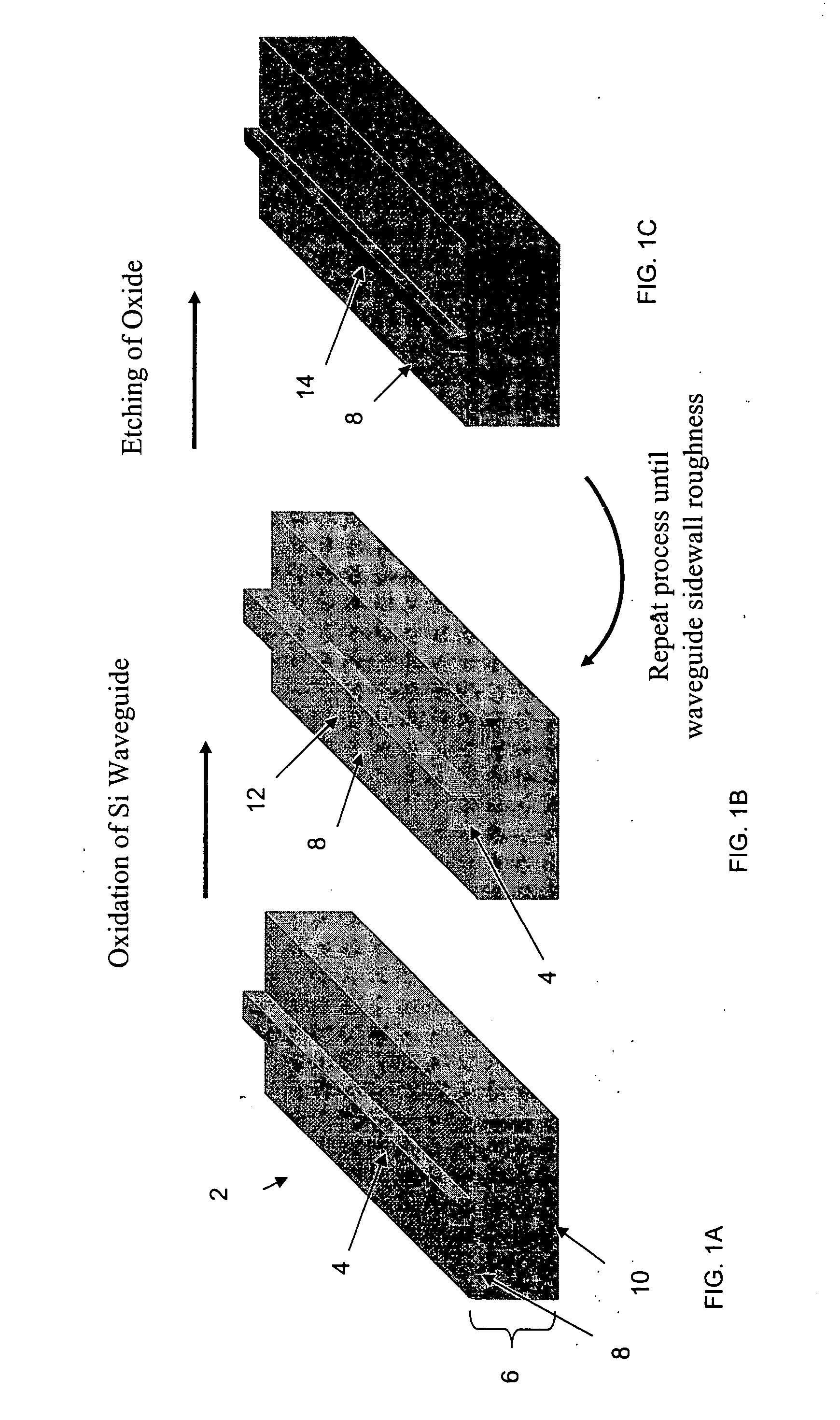
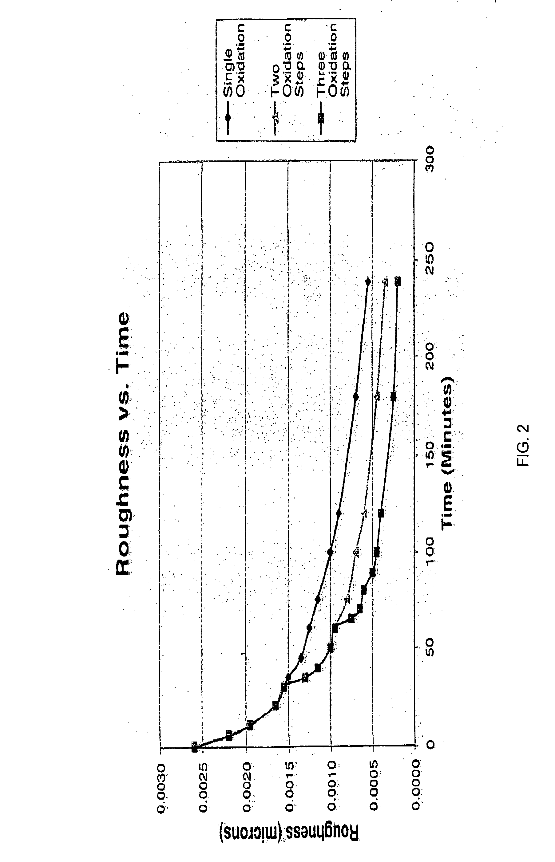
[0013] The invention is a novel processing method for reducing waveguide roughness in waveguides. While similar to oxidation smoothing, the inventive multiple oxidation smoothing method (MOSM) reduces oxidation time significantly by remaining in the fast, reaction-limited regime, rather than the slow, diffusion-limited regime.

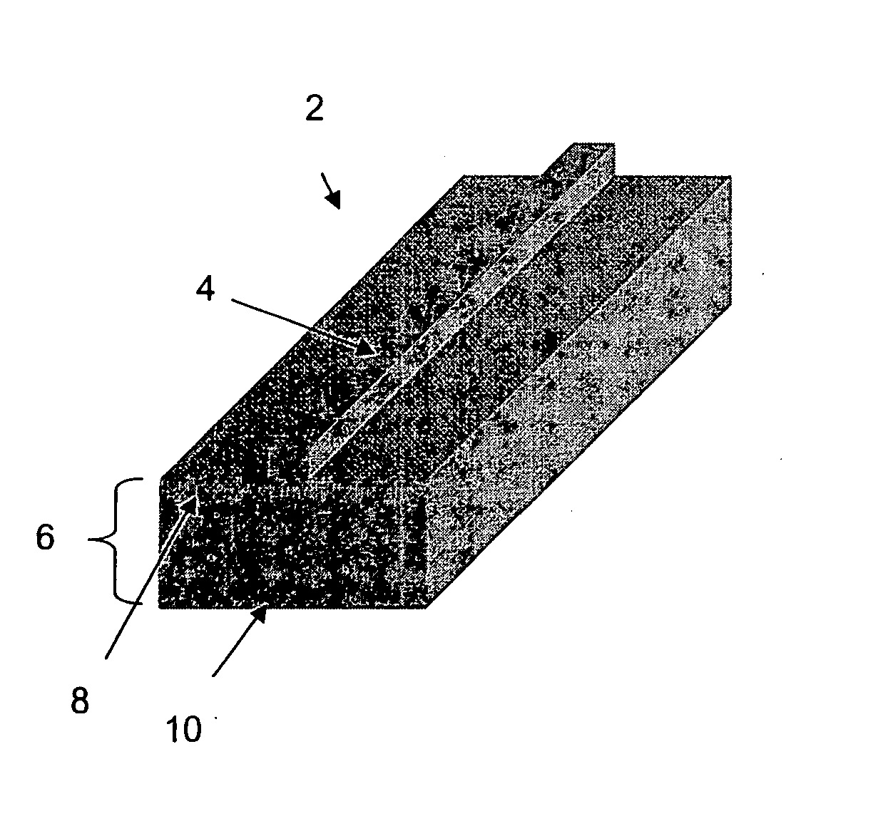
[0014]FIGS. 1A-1B illustrates the method steps taken to reduce waveguide roughness in accordance with the invention. FIG. 1A shows a Si waveguide 2 used in accordance with the invention. The Si waveguide 2 is formed by depositing a Si layer 4 on an oxidized Si wafer 6. The oxide layer 8 on a Si wafer 10 serves as the undercladding for the waveguide 2, which is comprised of low index material. The deposited top Si layer 4 is etched with a photolithography mask to define the waveguides. This leaves a waveguide with rough sidewalls on top of an oxide surface, which is above the Si wafer. The lower oxide cladding 8 is not touched by the MOSM process.

[0015] When a...


PUM


Abstract

The light-guiding structure includes a waveguide structure that comprises a substrate and a low refractive index underclad material. The waveguide structure is oxidized to form an oxidized layer on a surface of the waveguide structure. The oxidized layer is isotropically etched after the reaction-limited oxidation regime is approaching the diffusion-limited regime and repeatedly oxidized and etched so that the waveguide structure is continuously oxidized in the reaction-limited regime, reducing the overall time of oxidation and volume of oxidized material so that the waveguide structure has its sidewall roughness reduced efficiently enabling high transmission rates of guided light.

Description

PRIORITY INFORMATION [0001] This application claims priority from provisional application Ser. No. 60 / 478,747 filed Jun. 16, 2003, which is incorporated herein by reference in its entirety.BACKGROUND OF THE INVENTION [0002] The invention relates to the field of optical communication, and in particular to high transmission waveguides and magnetooptical isolators having high Faraday rotation that can be integrated on Si and GaAs substrates. [0003] Waveguides are typically made by deposition of the core material on a substrate of cladding material. Lithography is used to define the layout, of the waveguides, an etching step is used to pattern the waveguides, and finally a cladding is deposited on top. This typically leaves waveguides with minimal roughness on the top and bottom of the waveguide but substantial roughness on the sidewalls. There are currently two methods for reducing the roughness of silicon waveguides. [0004] The first involves using an anisotropic etch which preferenti...

Claims


Application Information

Patent Timeline
IPC IPC(8): G02B6/12G02B6/122G02B6/13G02B6/136
CPCG02B6/122G02B2006/12097G02B6/136G02B6/13
Inventor SPARACIN, DANIEL K.WADA, KAZUMIKIMERLING, LIONEL C.
Owner MASSACHUSETTS INST OF TECH
Why Eureka
Try Eureka