
Thin film integrated circuit device

a technology of integrated circuits and thin films, applied in the direction of coded identity cards or credit card actuation, organic semiconductor devices, instruments, etc., can solve the problems increased and increased risk of unauthorized use of ic cards

Inactive Publication Date: 2004-12-09
SEMICON ENERGY LAB CO LTD
View PDF24 Cites 49 Cited by
  • Summary
  • Abstract
  • Description
  • Claims
  • Application Information

AI Technical Summary

Benefits of technology

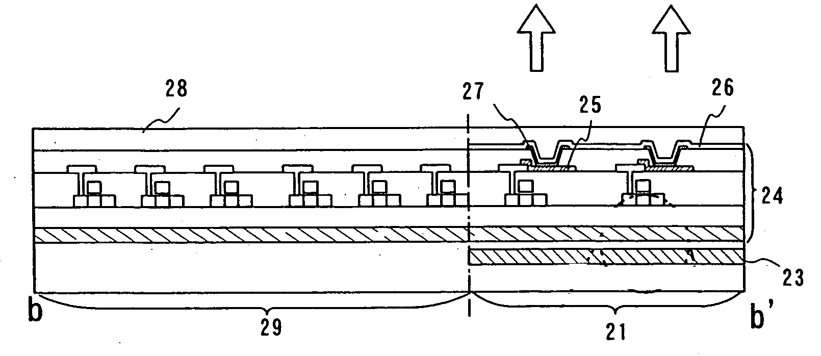
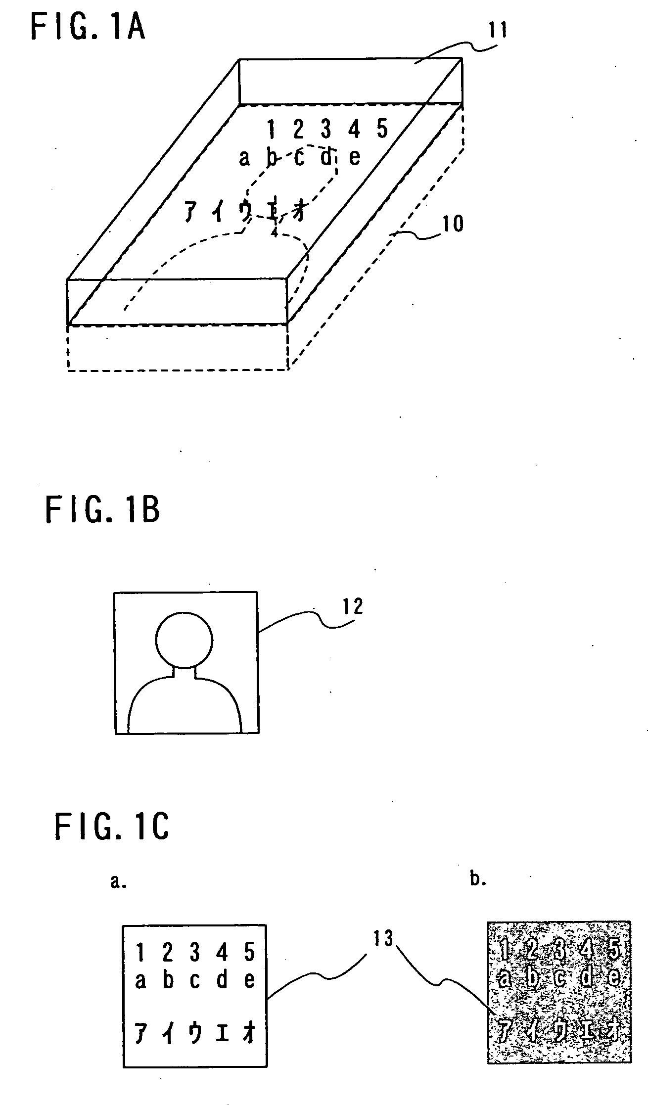
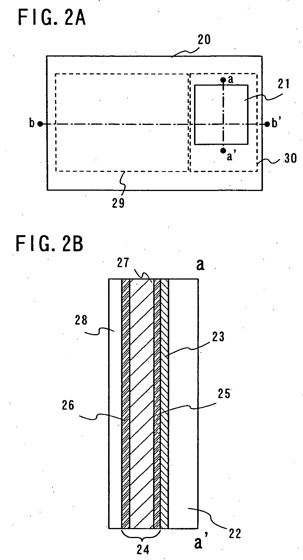
[0008] Considering the above objects, in a device including a thin film integrated circuit of the present invention (hereinafter referred to as a thin film integrated circuit device), a first display area and a second display area having transparency are provided and stacked together. According to the present invention, much information can be provided by stacking display of the first display (first display) and display of the second display area having transparency (second display), even if the display region has a little area. In other words, the area of the display region can be reduced.
[0014] Note that, a thin film integrated circuit of the present invention is a integrated circuit having a greatly thin semiconductor film as an active region. The thin film integrated circuit can be formed on a substrate having flexibility, which is made of a plastic material or the like (such a substrate is hereinafter referred to as a film substrate). On that account, the thin film integrated circuit of the present invention is far lighter compared with an integrated circuit formed on a conventional silicon wafer (so-called IC chip), it can be made thin, and it is hardly damaged even when it is dropped. Thus, the thin film integrated circuit of the present invention is suitable for a thin film integrated circuit device such as an IC card which requires lightweight, thinness of film, and high breaking strength. Further, a pixel area or a driver circuit area of a light-emitting device may be formed using the thin film integrated circuit of the present invention.
[0016] As thus described, the present invention can provide plural displays in a display area of a thin film integrated circuit device or a portable electronic device, and can provide much information.

Problems solved by technology

On the other hand, unauthorized use of IC cards increases and the countermeasure is urgently needed.
However, when a PIN number, a password, or a photograph of the face provided on a part of a card is used, in case of loss or theft, a person other than the identical person might tamper the contents and use the card illegally.
Further, the display area of a card is limited, and thus, the information that can be provided is limited.
Moreover, when a read / authentication system carrying a fingerprint scanner is used as disclosed in Reference 2, the cost of equipment becomes higher to introduce the necessary apparatus.

Method used


Image

  • Thin film integrated circuit device
  • Thin film integrated circuit device
  • Thin film integrated circuit device

Examples


embodiment mode 6

[0085] Embodiment Mode 6

[0086] In this embodiment mode, a manufacturing method of a thin film integrated circuit of the present invention, a method for forming a thin film transistor over a film substrate by using peeling and transfer techniques will be described.

[0087] First, a metal film 71 is formed over the first substrate 70 as shown in FIG. 7A. The first substrate should have rigidity that can withstand the following peeling step, for example, a glass substrate, a quartz substrate, a ceramic substrate, a silicon substrate, a metal substrate, or a stainless steel substrate may be used. For the metal film, a single layer of an element selected from W, Ti, Ta, Mo, Nd, Ni, Co, Zr, Zn, Ru, Rh, Pd, Os, and Ir, or an alloy material or a compound material which is based on the element; or a laminate thereof can be used. For an example of a method for forming a metal film, the metal film may be formed by sputtering using a metal target. The metal film may be formed to have a film thick...

embodiment

[0143] Embodiment Mode 8

[0144] A first display can use a static image (rest image) or a moving image (an animated image). A second display can also use a static image or a moving image. Accordingly, in this embodiment mode, combination of the first display area and the second display area having transparency will be described.

[0145] First, the case of using a static image for the first display and a moving image for the second display will be described. In the first display, a static image displayed by using a photograph, a liquid crystal display device, a light-emitting device (a display device including a light emitting element such as an EL element), electron paper, or the like can be used as described above. Further, a dual emission light-emitting device displaying a moving image can be used for the second display. When a static image is used for the second display, the dual emission light-emitting device may display the static image.

[0146] When a moving image is used for the fi...


PUM


Abstract

A device having an integrated circuit, especially an IC card, for reliably verifying a person's identity by display of PIN numbers or passwords with ingenuity. Portable electronic devices such as a PDA or a cellular phone, or other products can have plural displays in a display area (display part) provided in a limited area. A first display area and a second display area having transparency are stacked together in a thin film integrated circuit device of the present invention. The area of display can be reduced and display of more complicated PIN numbers or passwords is enabled by layering the display of the first display area and the display of the second display area.

Description

[0001] 1. Field of the Invention[0002] The present invention relates to a thin film integrated circuit device including an integrated circuit such as a microprocessor (CPU), a memory. The present invention particularly relates to an IC card or a portable electronic device typified by a PDA and a cellular telephone.[0003] 2. Description of the Related Art[0004] In recent years, as the field where an IC card is used is broaden, demand for an IC card having multifunctionality has been increasing. On the other hand, unauthorized use of IC cards increases and the countermeasure is urgently needed. An approach to the accurate personal-identification can be given as a countermeasure for the unauthorized use. As for a generally available IC card, the management using a personal identification number (PIN number) or a password, or printing a photograph of the face in a part of the card are given as methods for personal identification. Further, a method in which personal identification data s...

Claims


Application Information

Patent Timeline
IPC IPC(8): G07F7/08G07F7/10H01L29/76H01L31/036H01L31/112
CPCG06K19/07703G07F7/086G07F7/1008G07F7/1025H01L27/3244H01L51/5234H01L2251/5323H10K59/12H10K2102/3031H10K59/80524H10K50/828
Inventor YAMAZAKI, SHUNPEITACHIMURA, YUKOWATANABE, YASUKO
Owner SEMICON ENERGY LAB CO LTD
Learn More