
Ether monomers and polymers having multi-ring structures, and photosensitive polymers and resist compositions obtained from the same

a technology of ether monomers and polymers, applied in the field of photosensitive polymers, can solve the problems of many problems in practical use, limitation of forming such a fine pattern, and serious line edge roughness in pattern formation

Inactive Publication Date: 2004-09-02
SAMSUNG ELECTRONICS CO LTD
View PDF4 Cites 5 Cited by
  • Summary
  • Abstract
  • Description
  • Claims
  • Application Information

AI Technical Summary

Benefits of technology

The present invention relates to photosensitive polymers and photoresist compositions that can be used in the production of semiconductor and other microelectronic devices. The invention addresses the need for photosensitive polymers that can form fine patterns with high resolution and can resist dry etching, while also being cost-effective and easy to process. The invention proposes the use of photosensitive polymers that incorporate specific monomers and have a unique structure that enhances resistance to dry etching and improves pattern formation. The invention also addresses the issue of heavy metal catalyst residues in the resulting polymer product and proposes a solution to mitigate this risk.

Problems solved by technology

However, when a conventional photoresist material is exposed with KrF excimer laser (248 nm), there is a limitation in forming such a fine pattern.
Whereas research into ArF and F.sub.2 excimer laser techniques is being vigorously carried out, existing resist compositions suitable for use in those techniques cause many problems in practical use, compared to conventional KrF resist compositions.
However, the resistance to dry etching is generally less than satisfactory for fine patterning processes and tends to result in serious line edge roughness in patterns formed from resist layers including such polymers.
Another drawback of polymers having the formula above is that the raw materials used to synthesize the polymer is expensive.
Also, the copolymer has a glass transition temperature (T.sub.g) of 200.degree. C. or higher due to the structural strength of norbornene contained in the backbone, resulting in processing difficulty.
In addition, the synthetic polymers have in their backbone the alicyclic group, which shows prominent hydrophobicity, and thus the adhesiveness to neighboring material layers is very poor.
However, according to reports hitherto made, resistance to dry etching has not been enhanced very much.
However, the resulting resist still exhibits weak resistance to dry etching or poor patterns.
As the pattern rule becomes finer in the manufacture of semiconductor devices, the aspect ratio is considerably increased, resulting in the collapse of patterns.
Photoresists incorporating such polymers, however, tend to be hydrophobic, suffer from reduced adhesion and exhibit reduced transmittance, reducing their utility for forming fine patterns.
However, a portion of the heavy metal catalyst remains in the resulting polymer product even after purification.
As a result, photoresist compositions incorporating such polymers present a serious risk of heavy metal contamination and would not be practical for use in most semiconductor process applications.
that tend to exhibit improved transmittance as a result of the additional fluorine in the main chain, but also tend to have poor adhesion characteristics.
to provide additional improvements in transmittance, but these improvements tend to come at the expense of reduced resistance to dry etch processes and / or reduced adhesion.

Method used


Image

  • Ether monomers and polymers having multi-ring structures, and photosensitive polymers and resist compositions obtained from the same
  • Ether monomers and polymers having multi-ring structures, and photosensitive polymers and resist compositions obtained from the same
  • Ether monomers and polymers having multi-ring structures, and photosensitive polymers and resist compositions obtained from the same

Examples


polymer synthesis examples

Copolymer Synthesis Example 2-1

[0056] 24

[0057] T-butyl 3-oxa-tricyclo[6.2.1.0.sup.2,7]undec-4-ene-10-carboxylate (25 g), prepared according to Monomer Synthesis Example 1-1, and 2-trifluoromethylacrylate (15.0 g) were dissolved in tetrahydrofuran (THF) (100 g) and placed in a reactor, in this instance a 3-neck round-bottom flask, after which the reactor was purged with N.sub.2 gas. After adding 2,2'-azobisisobutyronitrile (AIBN) (2 mol %) to the reactor, the polymerization proceeded for a polymerization time of about 12 hours at a polymerization temperature of about 70.degree. C. under N.sub.2 purging to obtain a product solution. After terminating the polymerization, the reaction product was precipitated from the product solution slowly in excessive hexane and filtered to separate the precipitates. This first retentate was then dissolved in THF, re-precipitated in hexane and again filtered to separate the precipitates. The second retentate was then dried in a vacuum oven maintained...


PUM

PropertyMeasurementUnit
polydispersityaaaaaaaaaa

Abstract

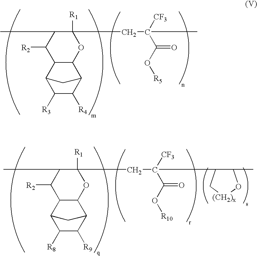
Provided are a variety of monomers suitable of producing photosensitive polymers, that are in turn, useful in photoresist compositions, through radical (cationic) polymerization including at least one multi-ring alkenyl ethers and one alpha-fluorinated acrylate. The resulting photoresist compositions exhibit both acceptable resistance to dry etching processing and light transmittance suitable for use with various light sources such as KrF excimer lasers, ArF excimer lasers or F2 excimer lasers, in a photolithography process to produce fine photoresist patterns. In addition to the multi-ring alkenyl ethers and alpha-fluorinated acrylates, additional monomers comprising one or more cyclic aliphatic and heterocyclic compounds, both unsubstituted and substituted, in particular dihydropyrans, may be incorporated into the photosensitive polymers. Photosensitive polymers can then be produced by combining these various monomer units to form copolymers, terpolymers and higher order polymers, an exemplary embodiment of which may be generally represented by the formula V:

Description

[0001] This application is a continuation-in-part and claims domestic priority from U.S. patent application Ser. No. 10 / 132,804, which was filed Apr. 24, 2002, in the U.S. Patent and Trademark Office, which is, in turn, based on and claims priority from Korean Patent Application No. 2003-85830, which was filed Nov. 28, 2003, in the Korean Intellectual Property Office, the disclosures of which are incorporated herein by reference in their entirety.[0002] 1. Field of the Invention[0003] The present invention relates to photosensitive polymers, and the production of such polymers, and photoresist compositions that incorporate such polymers that can be used in the production of semiconductor and other microelectronic devices. The photosensitive polymers are prepared by a method of radical (cationic) polymerization from at least two monomers including a multi-ring alkenyl ether and an .alpha.-fluorinated acrylate, and may further incorporate one or more cyclic aliphatic and heterocyclic ...

Claims


Application Information

Patent Timeline
Patent Type & Authority Applications(United States)
IPC IPC(8): C08F16/18C08F20/22C08F220/22G03F7/039C08F234/02G03F7/004G03F7/027
CPCC07D311/78C08F34/02G03F7/0046Y10S430/115Y10S430/106Y10S430/108G03F7/0395
Inventor KIM, HYUN-WOOWOO, SANG-GYUN
Owner SAMSUNG ELECTRONICS CO LTD
Learn More