Network conductor and its production method and use
a network conductor and conductor technology, applied in the field of network conductors, can solve the problems of poor energy efficiency and driving durability, uneven brightness, and the need for a higher driving voltage of the organic el device, and achieve the effects of low resistivity, high light transmittance, and excellent charge injection properties
- Summary
- Abstract
- Description
- Claims
- Application Information
AI Technical Summary
Benefits of technology
Problems solved by technology
Method used
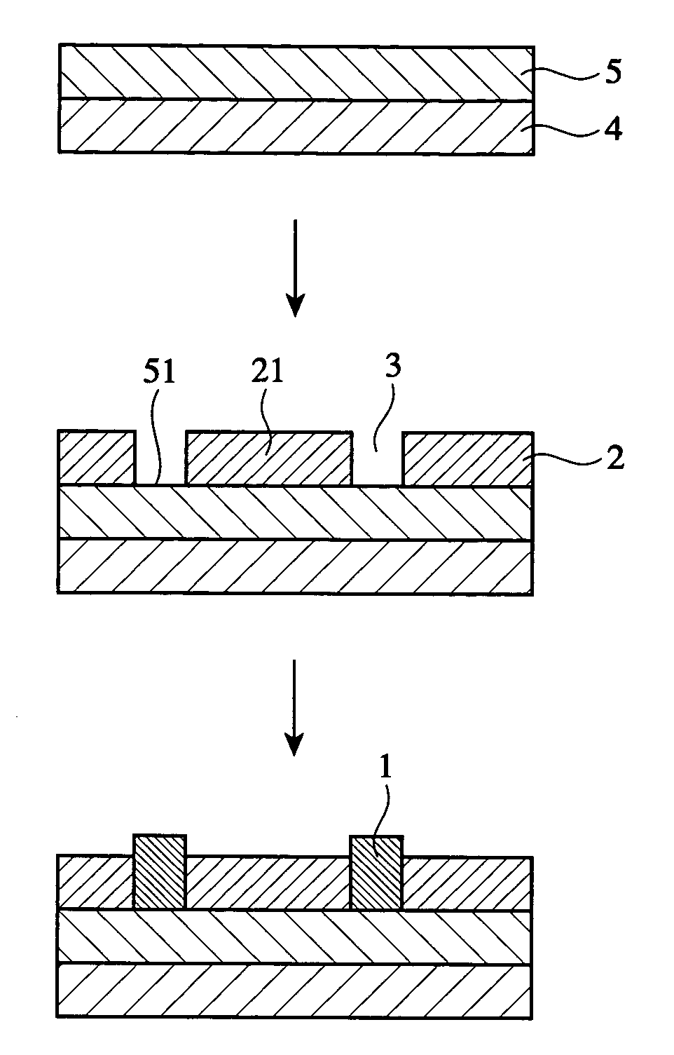
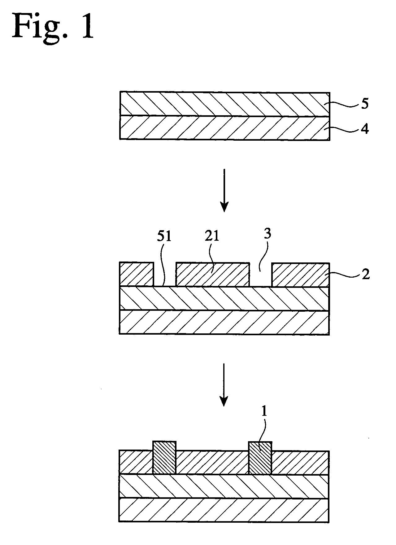
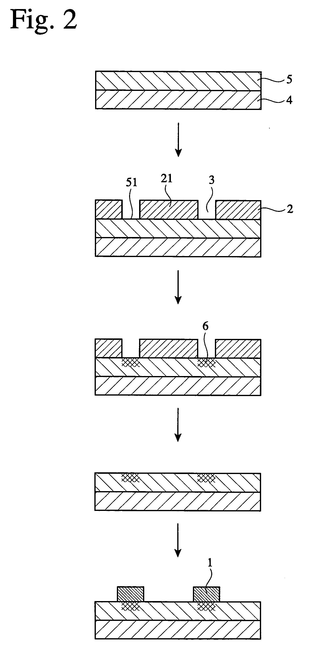
Image

Examples
example 2
[0181] Production of Organic EL Device
[0182] A transparent conductive layer of indium tin oxide (ITO, indium / tin=95 / 5 by mol) was formed into the 0.2 .mu.m thickness by a sputtering method using a direct-current power source on the sol-gel film containing the network conductor of the network conductor-having substrate obtained in Example 1. Thus, a positive electrode comprising the network conductor layer of silver and the transparent conductive layer of ITO was obtained. The positive electrode had the surface resistance of 4 .OMEGA. / square. A dichloroethane solution of a composition of polyvinyl carbazole / 1,1,4,4-tetraphenylbutadiene (blue light-emitting material) / tris(2-phenylpyridine) iridium complex (green light-emitting material of ortho-metallation complex) / 4-(dicyanomethylene-)-2-methyl-6-(4-dimethylaminostyryl)-4H-pyran (red light-emitting material) / 2-(4-biphenylyl)-5-(4-t-butylphenyl)-1,3,4-oxadiazole (electron-transporting material)=200 / 1 / 5 / 1 / 50 (weight ratio) was applied ...
example 3
[0186] Production of Network Conductor-Having Substrate
[0187] (1) Preparation of Bondable Underlayer
[0188] 1 g of 3-mercaptopropyltrimethoxysilane was added to 100 ml of an aqueous solution containing 1% by mass of acetic acid, and stirred to make the resultant mixture uniform. The obtained sol liquid was applied by a spin coater onto a glass substrate having a size of 0.7 mm in thickness.times.25 mm.times.25 mm, and heated at 120.degree. C. for 1 hour, to form a bondable underlayer.
[0189] (2) Preparation of Sol-Gel Film
[0190] A sol-gel film was formed on the bondable underlayer obtained in (1) in the same manner as in Example 1. The sol-gel film had the thickness of 0.4 .mu.m after drying. As a result of observing the sol-gel film by an optical microscope, the sol-gel film was cracked, and microcracks and domains surrounded by the microcracks were found.
[0191] (3) Preparation of Conductive Particles
[0192] An aqueous sodium citrate solution as a reducing agent was added to an aqueou...
example 4
[0195] Production of Organic EL Device
[0196] A transparent conductive layer of indium tin oxide (ITO, indium / tin=95 / 5 by mol) was formed in the 0.2 .mu.m thickness by a sputtering method using a direct-current power source on the sol-gel film containing the network conductor obtained in Example 3. Thus, a positive electrode comprising the network conductor layer of gold and the transparent conductive layer of ITO was obtained. The positive electrode had the surface resistance of 8 .OMEGA. / square and the light transmittance of 86% measured by a spectrophotometer. A light-emitting organic thin film having the thickness of 0.11 .mu.m was formed on the positive electrode in the same manner as in Example 2. Then, a negative electrode, which comprised a magnesium-silver alloy layer having the thickness of 0.25 .mu.m (mol ratio:magnesium / silver=10 / 1) and a silver layer having the thickness of 0.3 .mu.m, was formed on the light-emitting organic thin film in the same manner as in Example 2. ...
PUM
| Property | Measurement | Unit |
|---|---|---|
| work function | aaaaa | aaaaa |
| work function | aaaaa | aaaaa |
| work function | aaaaa | aaaaa |
Abstract
Description
Claims
Application Information
 - R&D
- Intellectual Property
- Life Sciences
- Materials
- Tech Scout
- Unparalleled Data Quality
- Higher Quality Content
- 60% Fewer Hallucinations
Browse by: Latest US Patents, China's latest patents, Technical Efficacy Thesaurus, Application Domain, Technology Topic, Popular Technical Reports.
© 2025 PatSnap. All rights reserved.Legal|Privacy policy|Modern Slavery Act Transparency Statement|Sitemap|About US| Contact US: help@patsnap.com