On-chip optical interconnection circuit, electro-optical device, and electronic apparatus

Inactive Publication Date: 2004-07-08
SEIKO EPSON CORP
View PDF5 Cites 12 Cited by
  • Summary
  • Abstract
  • Description
  • Claims
  • Application Information

AI Technical Summary

Problems solved by technology

The operation speed of the SOC is limited by problems of the signal delay or the increase of power consumption of such global wirings.
However, when optical fiber is used as an optical transmission device, connection with optical components, such as a light emitting element and a light receiving element, becomes complicated resulting in problems of enormous fabrication cost and fabrication time, and difficulty in minimizing the size of optical transm

Method used


Image

  • On-chip optical interconnection circuit, electro-optical device, and electronic apparatus
  • On-chip optical interconnection circuit, electro-optical device, and electronic apparatus
  • On-chip optical interconnection circuit, electro-optical device, and electronic apparatus

Examples


Embodiment Construction

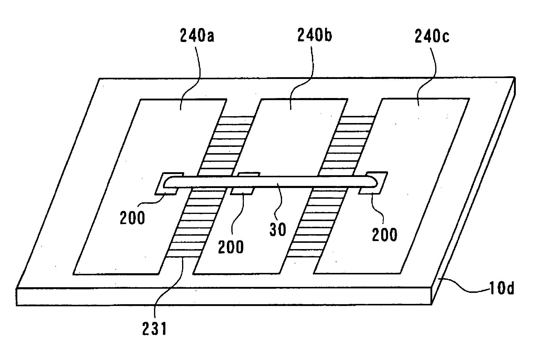
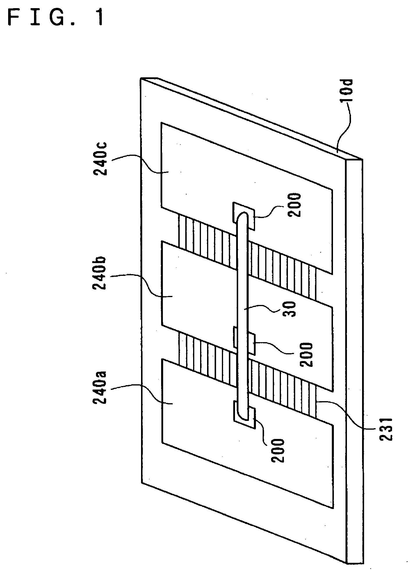
[0151] Hereinafter, an example of the application of the optical interconnection circuit according to an aspect of the present invention is described.

[0152] For example, the on-chip optical interconnection circuits of the above-described exemplary embodiments are used as signal transmission device of an optoelectronics integrated circuit system. A computer is an example of the optoelectronics integrated circuit system. Integrated circuits constituting a CPU are formed on the substrate 10 as TFT circuits, and integrated circuits constituting a storage device are formed on the substrate 10 as TFT circuits. Although signal processing in the integrated circuits constituting the CPU or the like is performed using electrical signals, the on-chip optical interconnection circuit of the above-described exemplary embodiments is applied to the data transmission between such TFT circuits.

[0153] As a result, in accordance with the present application example, it is possible to greatly enhance th...


PUM


Abstract

To provide an on-chip optical interconnection circuit, an electro-optical device, and an electronic apparatus, in which high signal transmission speed, easy miniaturization, and easy fabrication can be attained, there are provided a plurality of circuit blocks, which are provided on one integrated circuit chip, and an optical waveguide, which is provided on the integrated circuit chip to optically connect the circuit blocks to each other.

Description

[0001] 1. Field of Invention[0002] The present invention relates to an on-chip optical interconnection circuit, an electro-optical device, and an electronic apparatus.[0003] 2. Description of Related Art[0004] Originally, LSIs (Large Scale Integrated circuits) made progress as integrated circuits having specific functions, such as DRAM (Dynamic Random Access Memory) or MPU (Micro Processing Unit), but with the speedup of MPUs, SRAMs (Static Random Access Memories), used as high-speed cache memories, there has been increased integration into the same chip. Now, by integrating flash memory, DSP (Digital Signal Processor), DRAM, etc. into one chip, the LSIs are being developed into high-performance information processing systems.[0005] An LSI, where integrated circuits having such various functions are formed in the same chip, is called as a system-on-chip (SOC: System On Chip). In such SOC, integrated circuits (circuit blocks) having different functions are formed on one chip in a pla...

Claims


Application Information

Patent Timeline
IPC IPC(8): G02B6/12G02B6/122G02B6/138G02B6/42G02B6/43H01L27/15H01L31/0232H01S5/026H04B10/25H04B10/40H04B10/50H04B10/60H04B10/67H04B10/80
CPCG02B6/122G02B6/1221G02B2006/12104G02B6/4214G02B6/43G02B6/138
Inventor KONDO, TAKAYUKI
Owner SEIKO EPSON CORP
Why Eureka
Try Eureka