
Multilayer thin film hydrogen getter and internal signal EMI shield for complex three dimensional electronic package components

a technology of electronic package components and hydrogen getters, which is applied in the direction of lighting and heating apparatus, other domestic objects, and semiconductor/solid-state device details, etc., can solve the problems of reducing the performance and reliability of gallium arsenide (gaas) integrated circuits, unable to re-work the assembly, and unable to return false results, etc., to achieve no cost or time, small volume, and flexible application.

Inactive Publication Date: 2004-06-03
RAYTHEON CO
View PDF9 Cites 13 Cited by
  • Summary
  • Abstract
  • Description
  • Claims
  • Application Information

AI Technical Summary

Benefits of technology

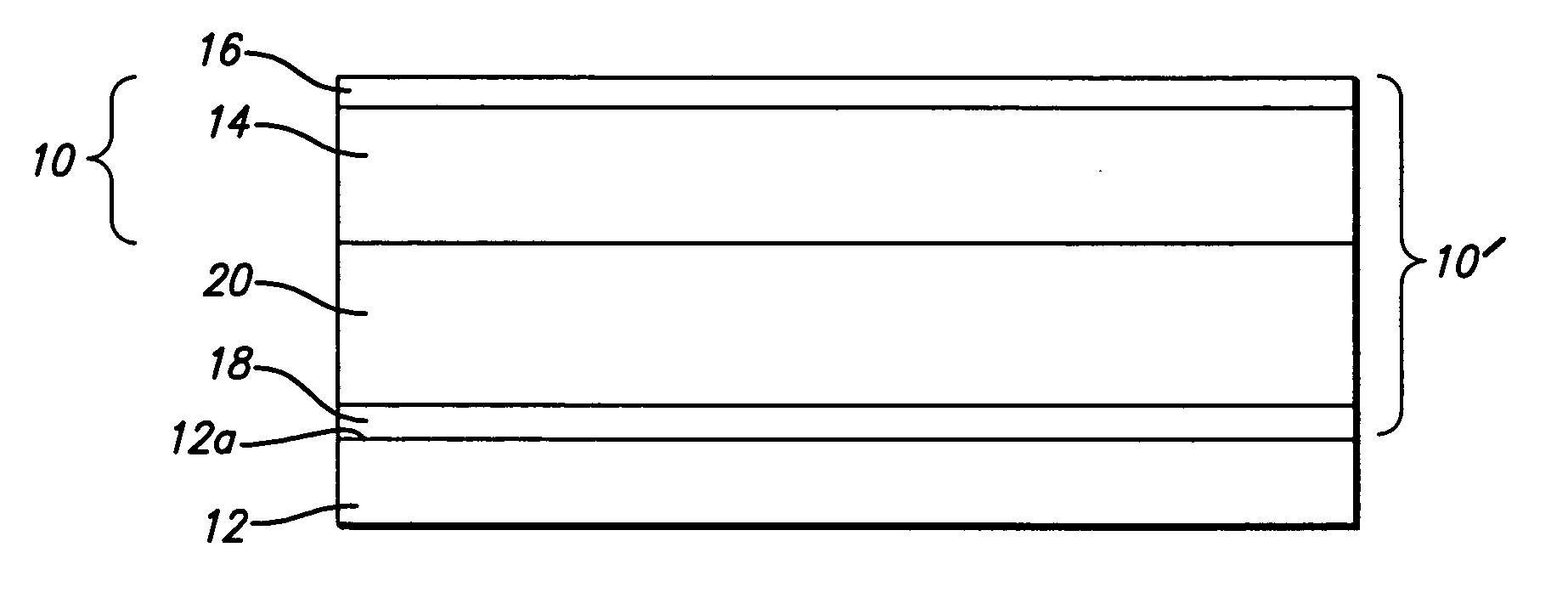
[0019] Both the titanium and the palladium are deposited during the same coating process (vacuum deposition) run, thereby preventing the titanium from being oxidized. The palladium continues to prevent the titanium from being oxidized once the getter is exposed to the atmosphere. However, hydrogen is easily able to diffuse through the palladium into the titanium where it is chemically bound up, since palladium is highly permeable to hydrogen. The present inventors have demonstrated high hydrogen absorption rates and hydrogen capacities for thin film getters deposited onto plastic test parts.
[0021] The thin film getter has several advantages: (1) Since the thin film getter has a hydrogen capacity per unit volume which is 25 times higher than the silicone getter, then the thin film getter will occupy an extremely small volume; (2) It is flexible in its application, since any convenient substrate that is going into the hermetic package can be coated with the thin film getter; (3) There is no cost or time associated with welding or bonding the thin film getter into the package as there is with foil or silicone getters; (4) The thin film getters don't require a lengthy vacuum bakeout prior to insertion; a vacuum bakeout of 85.degree. C. for 2 to 3 hours is sufficient; and (5) There is no silicone in the thin film getter, which prevents contamination.
[0022] In addition to the advantages that the thin film getter provides over the other getters, as described in greater detail below, the thin film getter is also able to absorb hydrogen effectively at temperatures as low as 0.degree. C.
[0023] The ground / EMI shield can be used to enhance circuit performance. The ground / EMI shield film component allows organic materials to be used within microwave modules, thereby providing cost benefits through reduced weight. The conductivity of the film allows its use in any type of dielectric package, thereby providing EMI and hydrogen protection for GaAs circuitry.

Problems solved by technology

Gallium arsenide (GaAs) integrated circuits which are hermetically packaged will suffer from reduced performance and reliability if the hydrogen that is evolved from the packaging materials is allowed to diffuse into the GaAs devices.
There are several disadvantages to this getter: (1) in order to provide enough hydrogen absorption capacity in a package, a significant volume of silicone getter must be used; (2) Residual Gas Analysis (RGA), used to determine internal contaminants within a hermetic package, can return false results related to moisture content when the silicone product is used; (3) silicone oil migration within the package has been observed, which makes re-work of the assembly impossible, due to the inability to re-solder joints wetted with the silicone oil; (4) there is added cost and complexity associated with having to bond the silicone getter sheet to some available surface; and (5) the silicone getter must first be vacuum baked at 150.degree. C. for greater than 16 hours before it can be inserted into the package.
This adds to the manufacturing time and cost.
These getters did not provide good reliable gettering capability, most likely due to the oxide layer present on the titanium foil.
A titanium foil would also have the added cost of welding to the package lid.
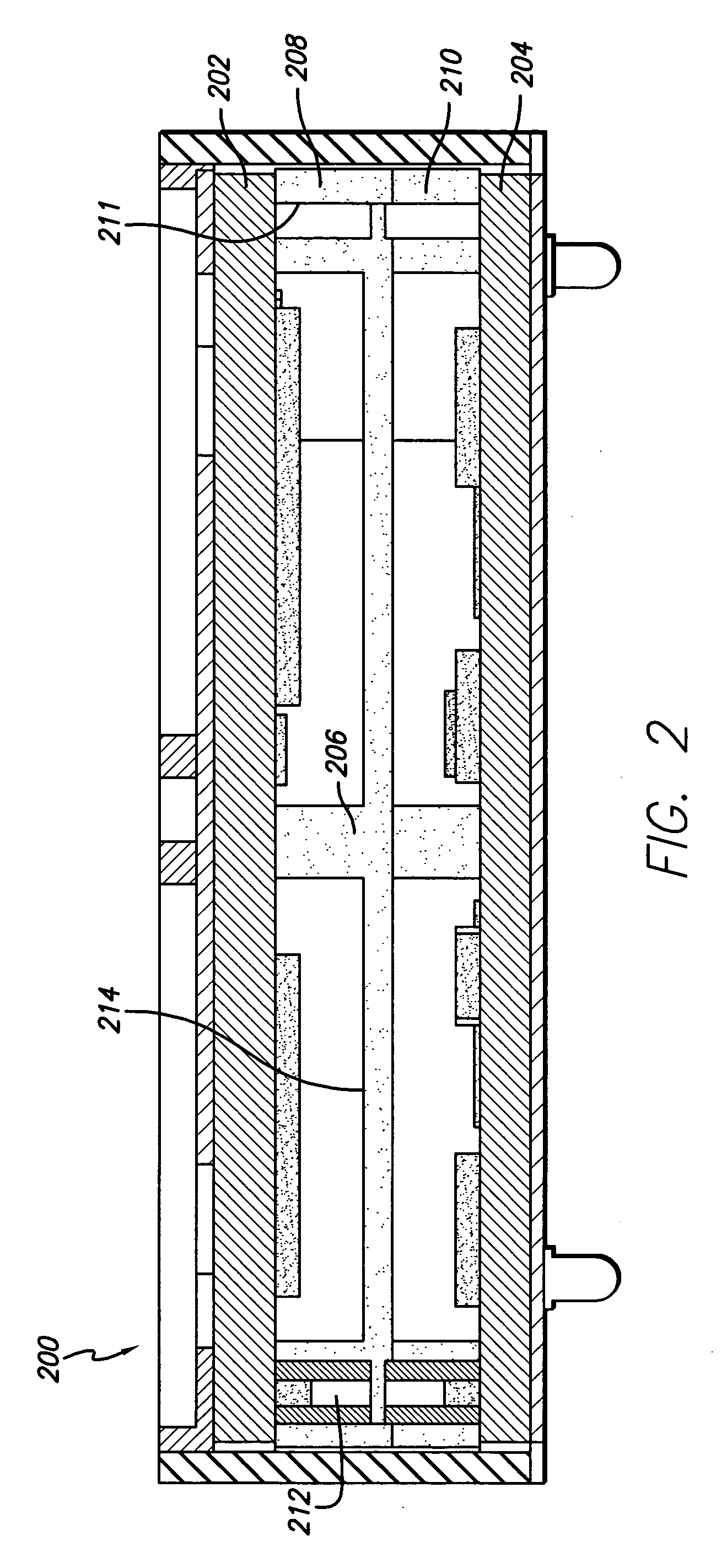
However, the cover in a 3-D package is now an electrically functional component and not suitable for location of a hydrogen-gettering material.
The reaction degradation of the film or gettering media cannot result in conductive particle generation, which would present functional risk to the packaged electronics.

Method used


Image

  • Multilayer thin film hydrogen getter and internal signal EMI shield for complex three dimensional electronic package components
  • Multilayer thin film hydrogen getter and internal signal EMI shield for complex three dimensional electronic package components
  • Multilayer thin film hydrogen getter and internal signal EMI shield for complex three dimensional electronic package components

Examples


Embodiment Construction

[0032] FIG. 1 depicts a conventional two-dimensional (2-D) module, which includes a cover that is an ideal location for an RF absorber material and a hydrogen absorber. The module 100 comprises a base 102, a cover 104 and a sealing ring 106 that seals the base to the cover. Inside the module 100, a substrate 108 is provided that supports a device 110, e.g., a Monolithic Microwave Integrated Circuit (MMIC) type, with a gallium arsenide (GaAs) semiconductor. On the inside of the cover 104 is provided a hydrogen gettering structure 112, typically comprising a titanium layer and a palladium layer thereon. The inside of the cover 104 may also include an RF absorbing material (not shown).

[0033] FIG. 1 amplifies the difference between conventional 2-D packaging and 3-D electronics with respect to the application of the prior art. It will be noted that the prior art is form fit with conventional 2-D packages. Since the cover 104 is simply used as a mechanism to close the package volume, it ...


PUM

PropertyMeasurementUnit
thicknessaaaaaaaaaa
thicknessaaaaaaaaaa
temperaturesaaaaaaaaaa

Abstract

A thin film hydrogen getter and EMI shielding are provided for protecting GaAs circuitry sealed in an hermetic package. The thin film getter comprises a multilayer metal film that is deposited by vacuum evaporation techniques onto a conductive metal, such as aluminum or copper, that serves as the EMI shielding. The conductive layer is first formed on an interior surface. The multilayer hydrogen getter film comprises (1) a titanium film and (2) a palladium film that is deposited on the titanium film. Both the titanium and the palladium are deposited during the same coating process run, thereby preventing the titanium from being oxidized. The palladium continues to prevent the titanium from being oxidized once the getter is exposed to the atmosphere. However, hydrogen is easily able to diffuse through the palladium into the titanium where it is chemically bound up, since palladium is highly permeable to hydrogen.

Description

[0001] The present application is a continuation-in-part application of application Ser. No. 09 / 965,759, filed Sep. 28, 2001.[0002] The present application is related to application Ser. No. 10 / 210,240, filed on Aug. 1, 2002, and entitled "Dielectric Interconnect Frame Incorporating EMI Shield and Hydrogen Absorber for Tile T / R Modules", the contents of which are incorporated herein by reference. That application is directed to dielectric interconnect frames, used in GaAs hermetically-sealed packaging.[0003] The present invention relates to packaging of gallium arsenide (GaAs) integrated circuits, and, more particularly, to a hydrogen getter for chemically binding up hydrogen evolved from packaging materials.[0004] Gallium arsenide (GaAs) integrated circuits which are hermetically packaged will suffer from reduced performance and reliability if the hydrogen that is evolved from the packaging materials is allowed to diffuse into the GaAs devices. By "packaging materials" is meant bas...

Claims


Application Information

Patent Timeline
Patent Type & Authority Applications(United States)
IPC IPC(8): F25B9/02H01L23/26
CPCH01L23/26H01L23/552H01L2924/1423Y10S428/938Y10T428/12569H01L2924/0002Y10T428/12806Y10T428/12875H01L2924/00H01L2924/1627
Inventor KOVACS, ALAN L.PETER, MATTHEW H.KETOLA, KURT S.LINDER, JACQUES F.
Owner RAYTHEON CO
Learn More