
Zirconia toughened ceramic components and coatings in semiconductor processing equipment and method of manufacture thereof

a technology of zirconia and ceramic components, which is applied in the field of high density plasma etching chambers for the fabrication of semiconductor wafers, can solve the problems of corrosion of various components of such equipment, cracking of coatings, shrinkage in both physical size and physical siz

Inactive Publication Date: 2004-02-05
LAM RES CORP
View PDF55 Cites 20 Cited by
  • Summary
  • Abstract
  • Description
  • Claims
  • Application Information

AI Technical Summary

Benefits of technology

The zirconia toughened ceramic coatings significantly reduce erosion and contamination, increase component lifespan, and maintain high mechanical strength and toughness, thereby improving the reliability and efficiency of semiconductor processing.

Problems solved by technology

Various components of such equipment are subject to corrosive conditions associated with semiconductor processing.
The '013 patent states that the differences in thermal expansion coefficients between aluminum and ceramic coatings such as aluminum oxide leads to cracking of the coatings due to thermal cycling and eventual failure of the coatings in corrosive environments.
As integrated circuit devices continue to shrink in both their physical size and their operating voltages, their associated manufacturing yields become more susceptible to particle and metallic impurity contamination.
Consequently, fabricating integrated circuit devices having smaller physical sizes requires that the level of particulate and metal contamination be less than previously considered to be acceptable.

Method used


Image

  • Zirconia toughened ceramic components and coatings in semiconductor processing equipment and method of manufacture thereof
  • Zirconia toughened ceramic components and coatings in semiconductor processing equipment and method of manufacture thereof
  • Zirconia toughened ceramic components and coatings in semiconductor processing equipment and method of manufacture thereof

Examples


Embodiment Construction

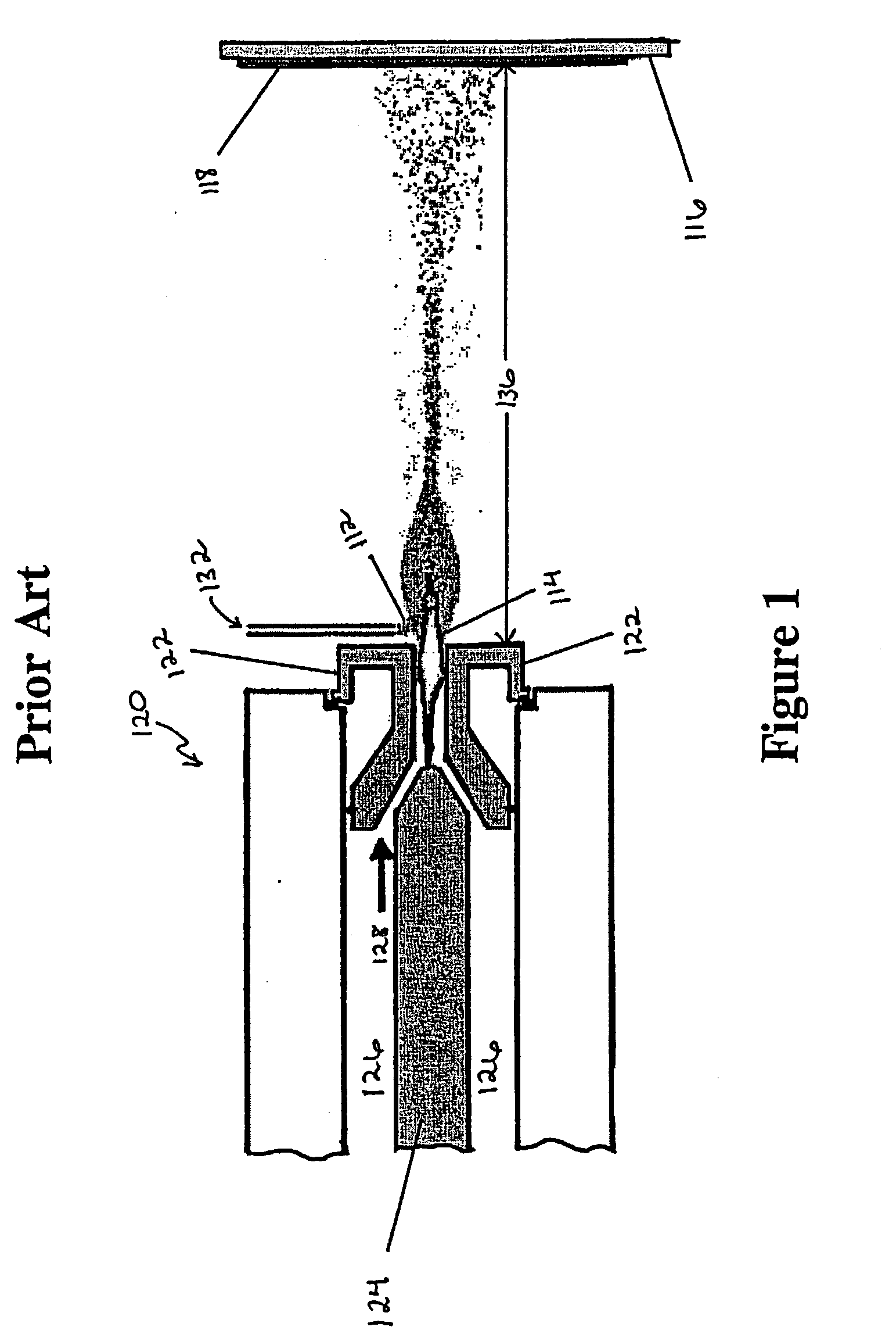
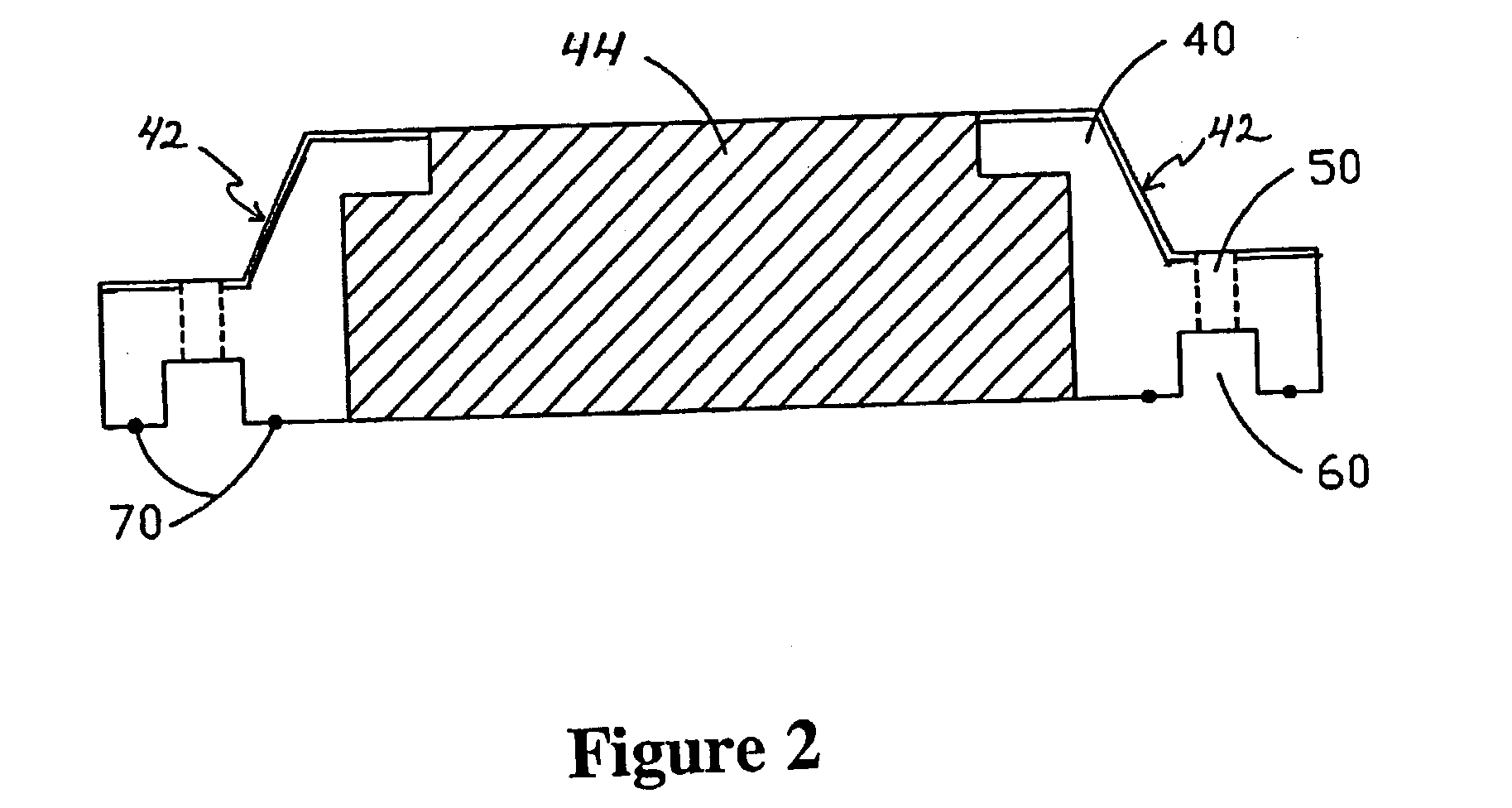
[0020] The present invention provides an effective way to provide corrosion resistance to the surfaces of components of semiconductor processing apparatus such as parts of a plasma processing reactor chamber. Such components include chamber walls, substrate supports, gas distribution systems (including showerheads, baffles, rings, nozzles, etc.), fasteners, heating elements, plasma screens, liners, transport module components, such as robotic arms, fasteners, inner and outer chamber walls, etc., and the like. In the present invention, the components themselves can be made from a zirconia toughened ceramic or the plasma exposed surfaces of the components can be coated or otherwise covered with a zirconia toughened ceramic material.

[0021] Zirconia toughened ceramic materials are a class of materials which utilize the tetragonal to mono-clinic phase transformation of metastable tetragonal zirconia particles to improve the strength and toughness of the ceramic. Under ambient pressure, z...


PUM

PropertyMeasurementUnit
melting pointaaaaaaaaaa
temperatureaaaaaaaaaa
distanceaaaaaaaaaa

Abstract

A corrosion resistant component of semiconductor processing equipment such as a plasma chamber comprises zirconia toughened ceramic material as an outermost surface of the component. The component can be made entirely of the ceramic material or the ceramic material can be provided as a coating on a substrate such as aluminum or aluminum alloy, stainless steel, or refractory metal. The zirconia toughened ceramic can be tetragonal zirconia polycrystalline (TZP) material, partially-stabilized zirconia (PSZ), or a zirconia dispersion toughened ceramic (ZTC) such as zirconia-toughened alumina (tetragonal zirconia particles dispersed in Al2O3). In the case of a ceramic zirconia toughened coating, one or more intermediate layers may be provided between the component and the ceramic coating. To promote adhesion of the ceramic coating, the component surface or the intermediate layer surface may be subjected to a surface roughening treatment prior to depositing the ceramic coating.

Description

[0001] 1. Field of the Invention[0002] The present invention relates generally to the fabrication of semiconductor wafers, and, more particularly, to high density plasma etching chambers having internal surfaces that reduce particle and metallic contamination during processing.[0003] 2. Description of the Related Art[0004] In the field of semiconductor processing, vacuum processing chambers are generally used for etching and chemical vapor depositing (CVD) of materials on substrates by supplying an etching or deposition gas to the vacuum chamber and application of an RF field to the gas to energize the gas into a plasma state. Examples of parallel plate, transformer coupled plasma (TCP.TM.) which is also called inductively coupled plasma (ICP), and electron-cyclotron resonance (ECR) reactors and components thereof are disclosed in commonly owned U.S. Pat. Nos. 4,340,462; 4,948,458; 5,200,232 and 5,820,723. Because of the corrosive nature of the plasma environment in such reactors an...

Claims


Application Information

Patent Timeline
Patent Type & Authority Applications(United States)
IPC IPC(8): C23C30/00C23C14/08C23C16/40H01J37/32H01L21/3065
CPCC23C14/083Y10T428/265H01J37/32477C23C16/405H01L21/67063
Inventor O'DONNELL, ROBERT J.CHANG, CHRISTOPHER C.DAUGHERTY, JOHN E.
Owner LAM RES CORP
Learn More