Cooper-plating solution, plating method and plating apparatus
- Summary
- Abstract
- Description
- Claims
- Application Information
AI Technical Summary
Benefits of technology
Problems solved by technology
Method used
Image
Examples
first embodiment
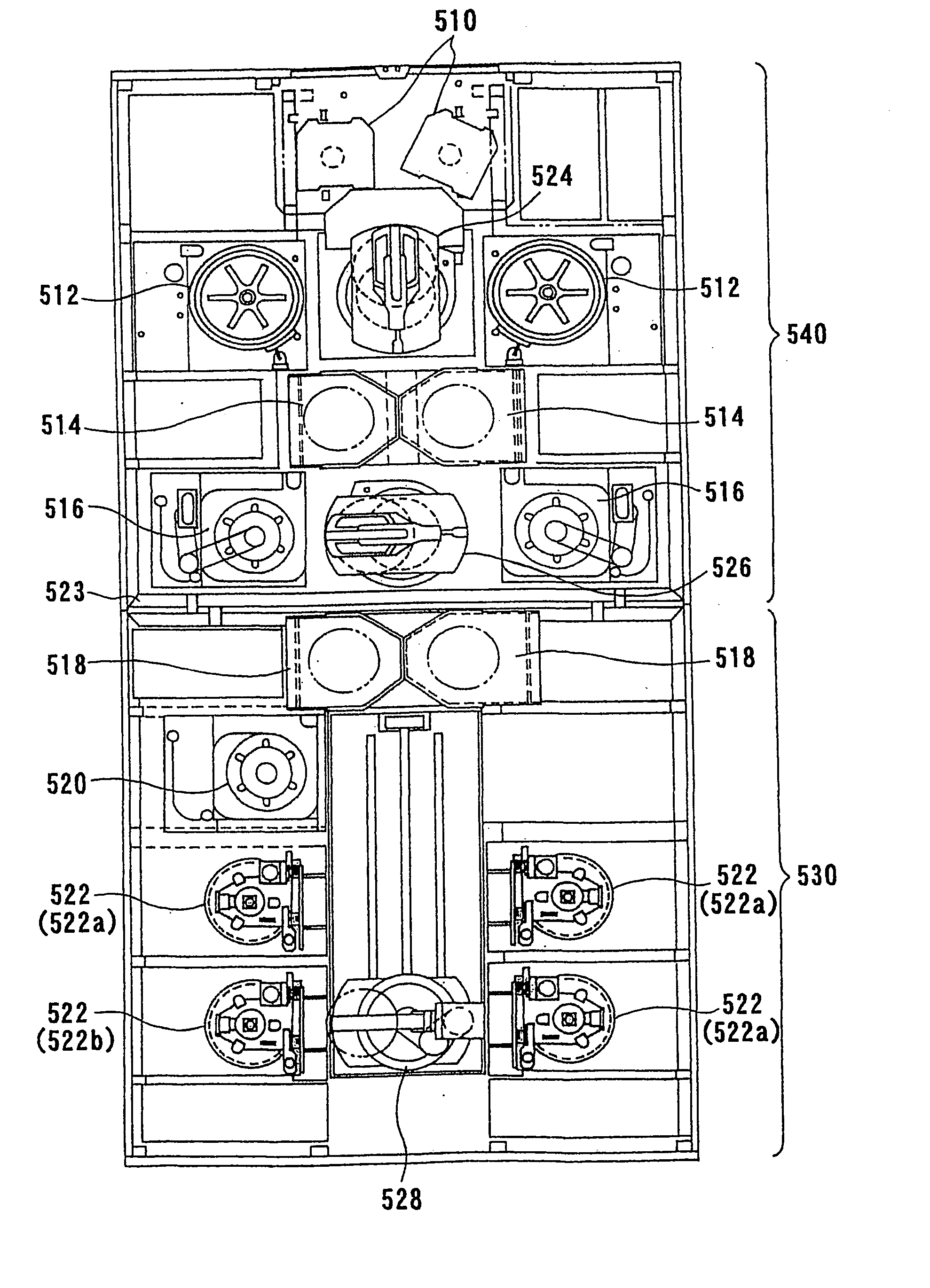
[0233] By using the copper-plating solution having the complex bath composition 1 (the present plating solution) as the copper-plating solution to be used in the first plating section 522a according to the present invention, a first-stage plating (reinforcement of seed layer) was carried out at a current density of 0.5 A / dm.sup.2 for 25 seconds. Thereafter, by using the copper-plating solution having the copper sulfate bath composition 1 as the copper-plating solution for the second plating section 522b, a second-stage plating (filling with copper) was carried out at a current density of 2.5 A / dm.sup.2 for 2 minutes.
[0234] The SEM observation revealed no voids in all of the via holes present in the entire surface of the substrate.
example 2
[0235] By using the copper-plating solution having the complex bath composition 2 (the present plating solution) as the copper-plating solution to be used in the plating section 522 according to the second embodiment of the present invention, plating (filling with copper) was carried out at a current density of 1 A / dm.sup.2 for 5 minutes.
[0236] The SEM observation revealed a few seam voids in certain via holes present in the peripheral region of the substrate.
example 3
[0237] By using the copper-plating solution having the complex bath composition 3 (the present plating solution) as the copper-plating solution to be used in the first plating section 522a according to the first embodiment of the present invention, a first-stage plating (reinforcement of seed layer) was carried out at a current density of 0.5 A / dm.sup.2 for 25 seconds. Therefore, by using the copper-plating solution having the copper sulfate bath composition 2 as the copper-plating solution for the second plating section 522b, a second-stage plating (filling with copper) was carried out at a current density of 2.5 A / dm.sup.2 for 2 minutes.
[0238] The SEM observation revealed no voids in all of the via holes present in the substrate.
PUM
| Property | Measurement | Unit |
|---|---|---|
| Density | aaaaa | aaaaa |
| Density | aaaaa | aaaaa |
| Density | aaaaa | aaaaa |
Abstract
Description
Claims
Application Information
 - R&D
- Intellectual Property
- Life Sciences
- Materials
- Tech Scout
- Unparalleled Data Quality
- Higher Quality Content
- 60% Fewer Hallucinations
Browse by: Latest US Patents, China's latest patents, Technical Efficacy Thesaurus, Application Domain, Technology Topic, Popular Technical Reports.
© 2025 PatSnap. All rights reserved.Legal|Privacy policy|Modern Slavery Act Transparency Statement|Sitemap|About US| Contact US: help@patsnap.com


