High-frequency wiring board
- Summary
- Abstract
- Description
- Claims
- Application Information
AI Technical Summary
Benefits of technology
Problems solved by technology
Method used
Image

Examples
Embodiment Construction
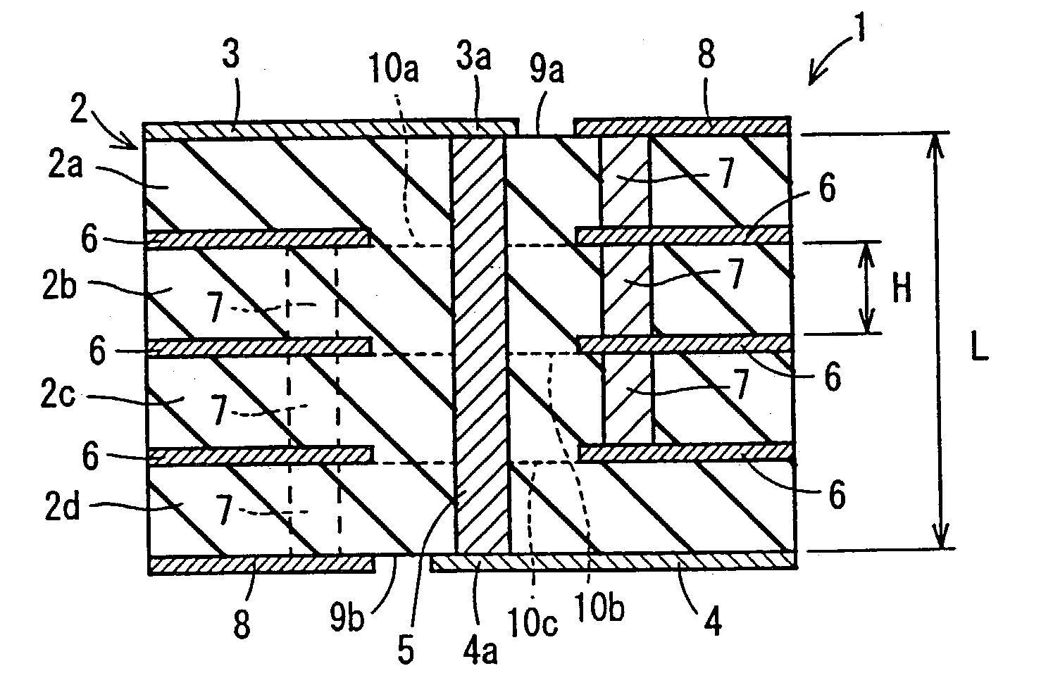
[0054] Next, a working example of the high-frequency wiring board of the invention will be explained below.
[0055] In a high-frequency wiring board 1, on upper and lower faces 9a, 9b of a dielectric board 2 formed by laminating four layers including dielectric layers 2a to 2d made of alumina ceramics having a dielectric constant of 8.6 and a thickness of 0.2 mm, as a first line conductor 3 and a second line conductor 4, line conductors made by adhering an Ni plating layer and an Au plating layer on a W metalize layer having a line width of 0.12 mm are formed, respectively. Moreover, almost entirely on the upper and lower faces 9a, 9b of the dielectric board 2, as the same plane ground conductors 8, conductors made by adhering Ni plating layers and Au plating layers on W metalize layers are formed with spaces of 0.1 mm so that characteristic impedance of the first line conductor 3 and the second line conductor 4 becomes 50 .OMEGA.. A through conductor 5 which connects one end 3a of th...
PUM
 Abstract
Description
Claims
Application Information
 - R&D
- Intellectual Property
- Life Sciences
- Materials
- Tech Scout
- Unparalleled Data Quality
- Higher Quality Content
- 60% Fewer Hallucinations
Browse by: Latest US Patents, China's latest patents, Technical Efficacy Thesaurus, Application Domain, Technology Topic, Popular Technical Reports.
© 2025 PatSnap. All rights reserved.Legal|Privacy policy|Modern Slavery Act Transparency Statement|Sitemap|About US| Contact US: help@patsnap.com