
Method for the formation of RF antennas by demetallizing and RF antenna products formed thereby

a technology of rf antenna and rf antenna, which is applied in the field of radio frequency tagging, can solve the problems of limiting the range of applications of the known system, unable to provide for the production of rf antennas of varying densities, and less flexible tag or label

Inactive Publication Date: 2002-09-19
NANOGRAFIX
View PDF2 Cites 58 Cited by
  • Summary
  • Abstract
  • Description
  • Claims
  • Application Information

AI Technical Summary

Benefits of technology

[0012] This invention thus provides an improved method of designing antennas on film or paper webs for use in radio frequency identification and / or tracking. Specifically, this invention uses a film or paper web, which is metallized on one or both sides, and demetallizes the antenna pattern on one or both of the metallized sides. This process uses a very thin layer of metal (usually 0.02-0.06 .mu.m) and demetallizes the antenna design or pattern in a uniform density or different densities in the same antenna if required. Because the web thickness is on the order of 25-50 .mu.m, the addition of the antenna has no significant effect on the thickness, and therefore the flexibility, of the web material as a tag or label. Further, there is no requirement for lamination to a label or tag because the antenna is created by demetallizing the area around the antenna design right on the web surface which will later be cut into labels or tags. The preprinted or plain label or tag web with its printed, holographic, optical variable device, diffractive, dot matrix, computer-generated holograms or computer-generated optical images on one side becomes the only substrate required to carry the antenna with its radio frequency circuit on the other side.
[0014] This invention therefore provides a method for demetallizing the antenna design on a metallized preprinted film or paper web used for creating labels, tags or packaging. This results in lower cost to produce the RF devices and increases the number of potential applications because of reduced label thickness and weight. Cost is reduced because there are fewer manufacturing steps required and fewer material costs. If the application is flexible or rigid packaging, then the antenna can be demetallized right on the material itself without further processing steps. If the application is a label or tag, the resulting label or tag is flexible, because it consists of only the film or paper with an adhesive backing. The liner is peeled from the back when applying the label or tag to the item to be tracked or read.
[0015] This invention represents an improvement over the prior art in several ways. It simplifies the manufacturing process for RF devices. Only one substrate is required for this process, which can be any type of film, paper, or other web material. It also reduces the cost of producing RF devices because of the reduction in material costs and the elimination of production steps. Less metal is deposited and yet can produce any type of antenna, and the need for additional material laminated to the antenna is eliminated.
[0016] In addition, because the lamination process is eliminated and only one substrate is required, the tag or label produced is extremely thin and flexible. This creates a tag or label flexible enough for use in variety of both flexible and rigid packaging materials. For example, a flexible RF label can be applied to a bottle or box as a seal or authentication device and it will conform to the package because of its flexibility.

Problems solved by technology

None of the known systems provides for production of antennas of varying densities.
Such a thickness creates a less flexible tag or label and restricts its range of applications.
In this process, the resulting thickness still reduces the flexibility and applicability of the tag or label.
None of these methods provides an approach to the design and fabrication of RF antennas that reduces cost, thickness, and weight of the antenna tag or label that also increases its flexibility to allow for a virtually unlimited number of applications.

Method used


Image

  • Method for the formation of RF antennas by demetallizing and RF antenna products formed thereby
  • Method for the formation of RF antennas by demetallizing and RF antenna products formed thereby
  • Method for the formation of RF antennas by demetallizing and RF antenna products formed thereby

Examples


Embodiment Construction

[0033] The invention is best understood by reference to the drawings. In the basic process of this invention, a film or paper web, which may or may not contain preprinted or embossed images upon it, and which is metallized on one or both sides, is sent through a demetallization process on a printing press to create RF antenna(s) on one or both sides of the web.

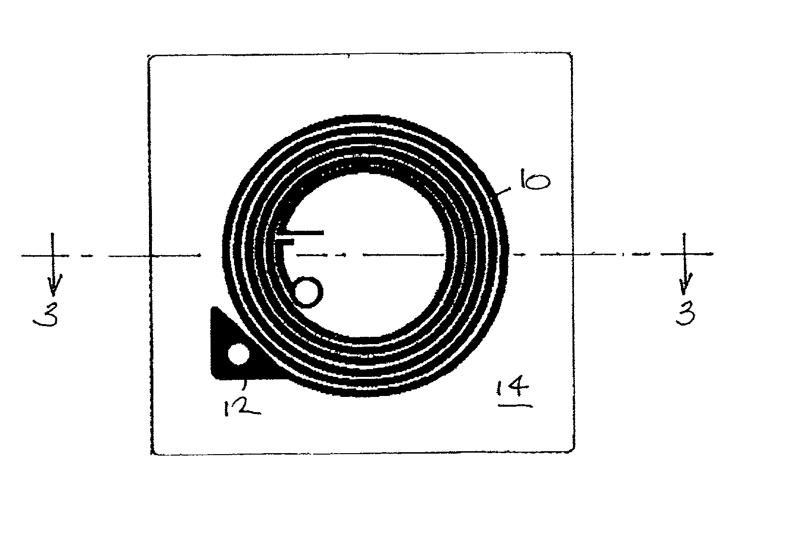
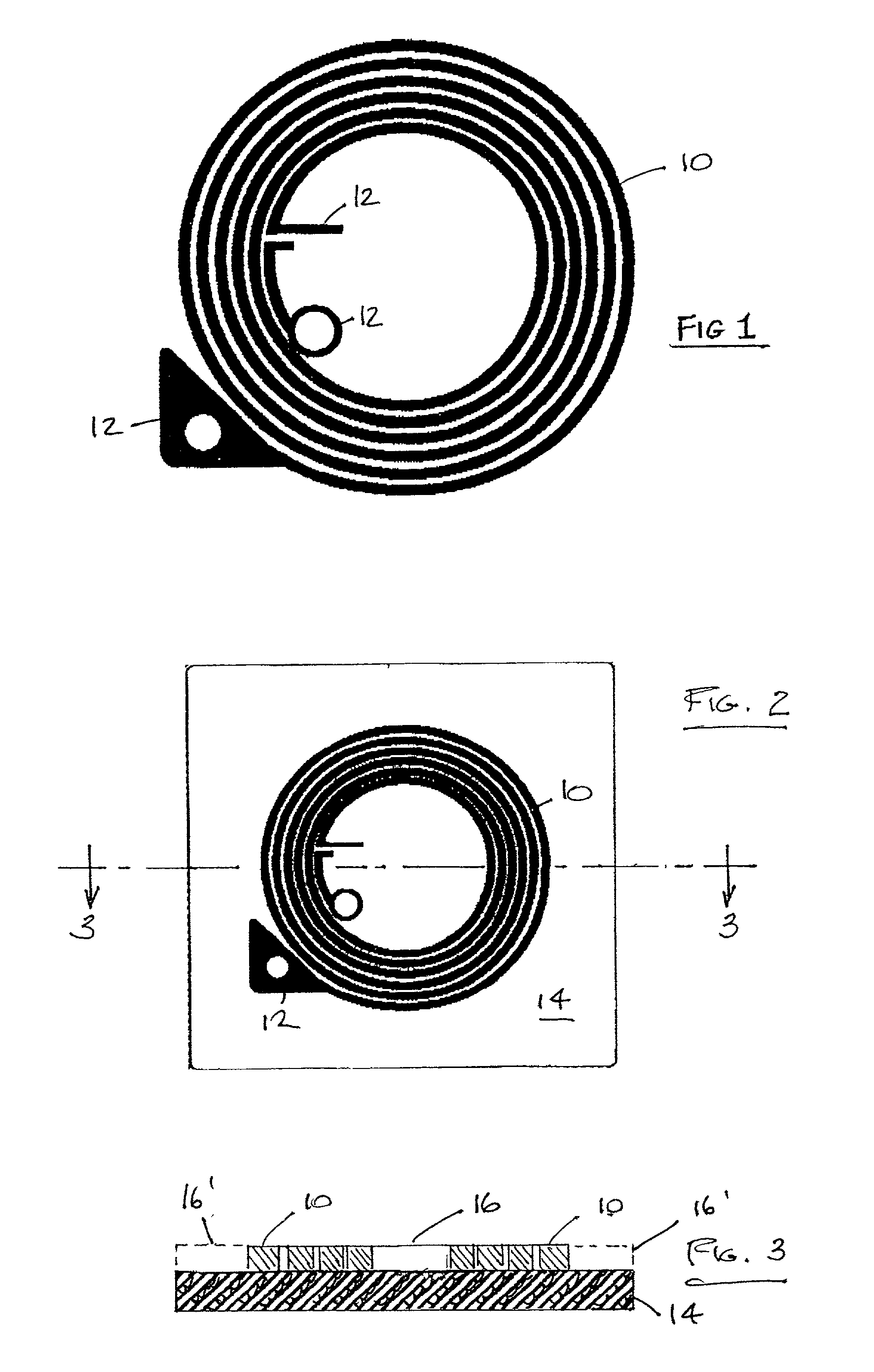
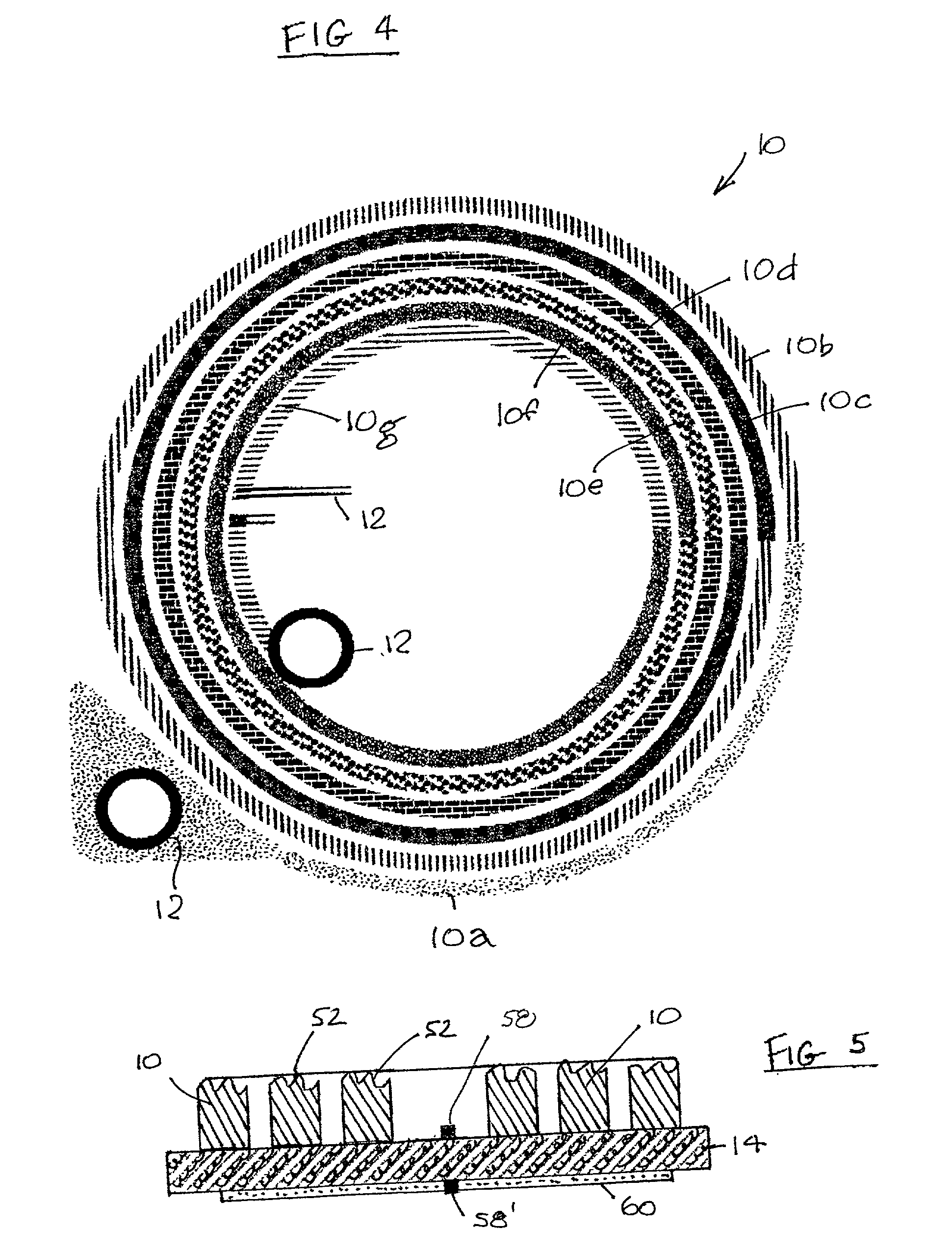
[0034] FIG. 1 is a plan view of a radio frequency (RF) antenna 10 which contains junction areas 12 for connection to conventional RF antenna circuitry. FIG. 2 is a plan view of the RF antenna 10 of FIG. 1 tag formed by demetallization on the surface of a substrate 14, in the manner to be described below. The substrate 14 will be a paper or film web and which contains a metallized layer 16 (see FIG. 7) on one or both sides, from which the RF antenna(s) are formed. The combination of the web and the antenna(s) can be used for conventional RF tags or labels. The metal 16 used for metallization of the web material can be aluminum,...


PUM

PropertyMeasurementUnit
thicknessaaaaaaaaaa
thicknessaaaaaaaaaa
thicknessaaaaaaaaaa

Abstract

A thin and flexible radio frequency (RF) antenna tag or label is disclosed which contains an RF circuit connected to an antenna which is created by demetallizing the area around the antenna pattern on a thin, metallized substrate such as a film or paper web. Antenna(s) may be formed on one or both sides of the substrate and can contain printed, holographic, optical variable device, diffractive, dot matrix, computer-generated holograms or computer-generated optical images. The demetallized RF antenna on the substrate can optionally further be transferred to a second substrate or web by means of a cold foil stamping process. The tag or label is thin and flexible, enabling a wide range of applications including RF tagging of anti-theft devices, product packaging of all types, credit cards, passports, admission tickets, stamps, vehicles, badges, fare cards, roadway tolls, customs and immigration checkpoints identification, and animal identification / tracking devices.

Description

[0001] 1. Field of the Invention[0002] This invention relates to the field of radio frequency (RF) tagging. More specifically, the invention relates to an improved method for creating an RF antenna on a lightweight, flexible substrate through demetallization of the substrate around the antenna pattern, leaving the metallized antenna.[0003] 2. Background of the Invention[0004] Radio frequency (RF) tagging or identification is one of many technologies for identifying and / or tracking objects. The RF identification process requires that information be carried on a substrate such as a tag or label containing an antenna. The antenna allows reception and transmission of radio waves. Typically, the tag or label containing the antenna reflects an incident RF carrier back to a base station. It radiates or receives energy and can be structured to radiate or receive energy over varying bandwidths.[0005] The tag usually consists of a semiconductor chip containing RF circuits, logic and memory an...

Claims


Application Information

Patent Timeline
Patent Type & Authority Applications(United States)
IPC IPC(8): H01Q1/38G06K19/077H01Q1/22
CPCG06K19/07718G06K19/07749G06K19/07779G06K19/07783G06K19/07784H01Q1/22H01Q1/2225H01Q1/38Y10T29/4902Y10T29/49018Y10T29/49156Y10T29/49016Y10T29/49798Y10T29/49073
Inventor LIEBERMAN, DANIEL
Owner NANOGRAFIX
Learn More