Semiconductor device and wiring method thereof

a technology of semiconductor devices and semiconductors, applied in the direction of semiconductor devices, semiconductor/solid-state device details, electrical apparatus, etc., can solve the problems of high risk of conventional semiconductor devices, inability to obtain the desired withstand voltage,

Inactive Publication Date: 2001-05-31
ROHM CO LTD
View PDF0 Cites 1 Cited by
  • Summary
  • Abstract
  • Description
  • Claims
  • Application Information

AI Technical Summary

Benefits of technology

[0008] Another transistor 14 is formed on the semiconductor device separately from the transistor 12 via a field oxide film 18 for component separation. Thus, by interposing the field oxide film 18 between the two transistors 12 and 14, it is possible to separate the transistors electrically.
[0011] To electrically separate the transistor 12 and the transistor 14 to avoid this situation, a sufficiently large length L1 of the non-inverted part can be secured. However, with this method, the overall length L2 of the field oxide film 18 becomes long, so the layout space for the transistor 12 and the transistor 14 becomes large. This leads to a reduction in the degree of integration of the semiconductor device.
[0013] Also, if the film thickness of the field oxide film 18 is increased, a greater time is required for forming the field oxide film 18, so production efficiency is lowered, and production costs are increased.
[0015] An object of the present invention is to provide a semiconductor device that solves these types of problems and that can separate components easily.

Problems solved by technology

However, such conventional semiconductor devices have the following type of problems.
There is a particularly high risk for this with high withstand voltage transistors for which a high voltage is applied to the gate electrode 22.
This makes it impossible to obtain the desired withstand voltage.
However, if the density of the channel stop ions is increased, there is a decrease in the withstand voltage.

Method used


Image

  • Semiconductor device and wiring method thereof
  • Semiconductor device and wiring method thereof
  • Semiconductor device and wiring method thereof

Examples


Embodiment Construction

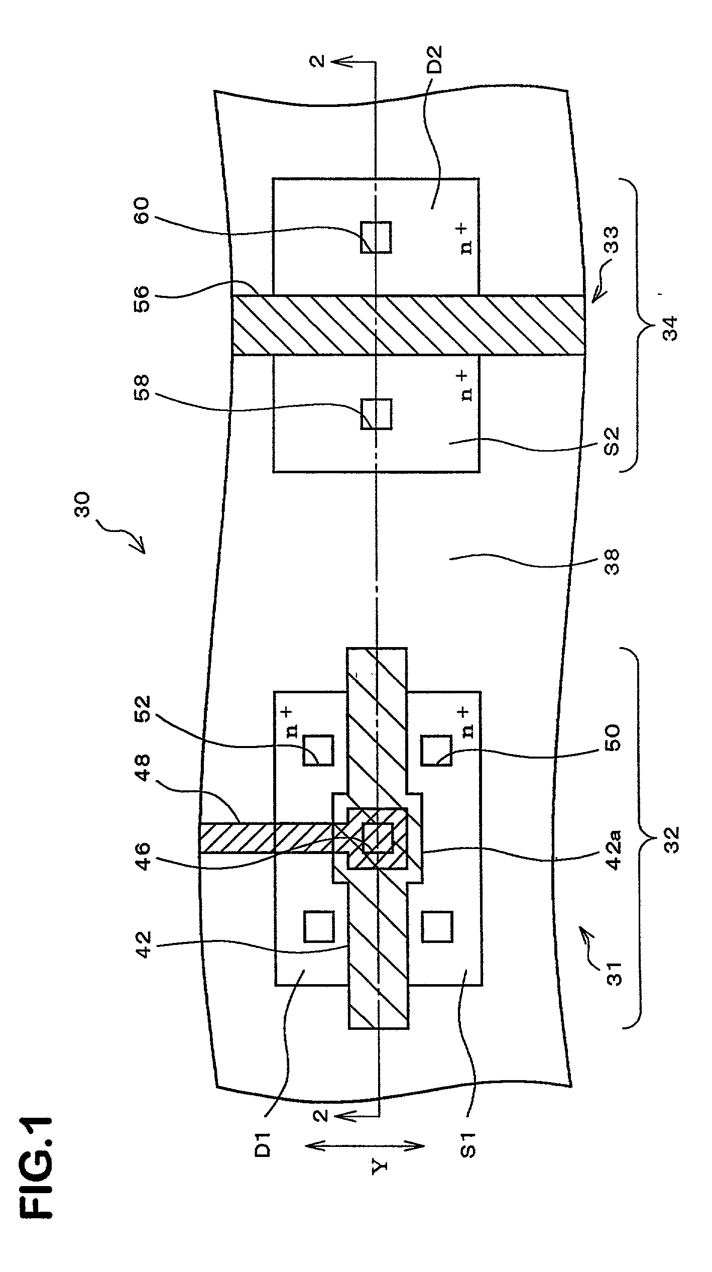
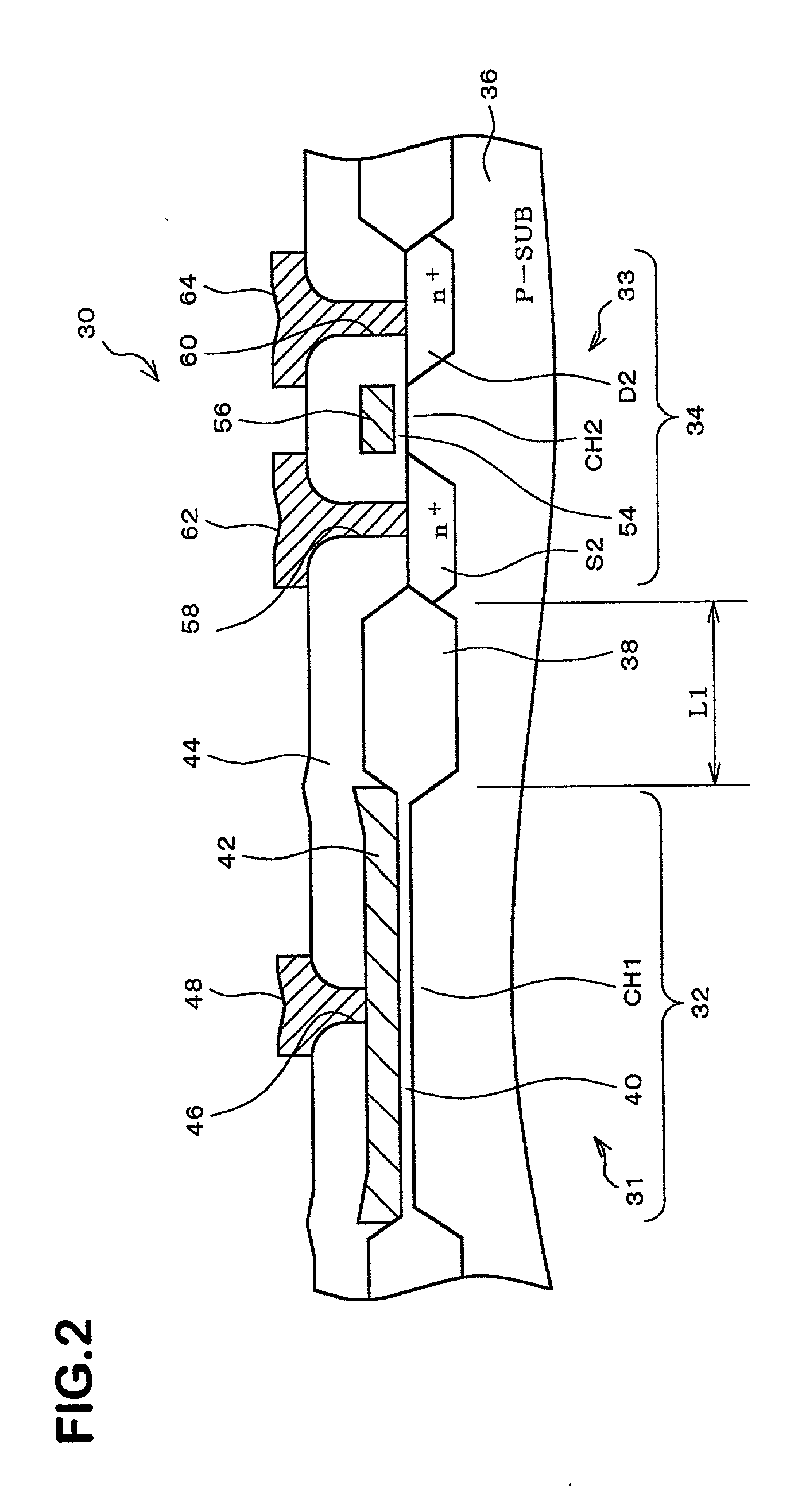
[0038] FIG. 1 conceptually illustrates a flat structure of a semiconductor device 30 which is a semiconductor device according to an embodiment of the present invention and which comprises a transistor 31 (semiconductor component). FIG. 2 is a cross-sectional view taken along line 2-2 of FIG. 1.

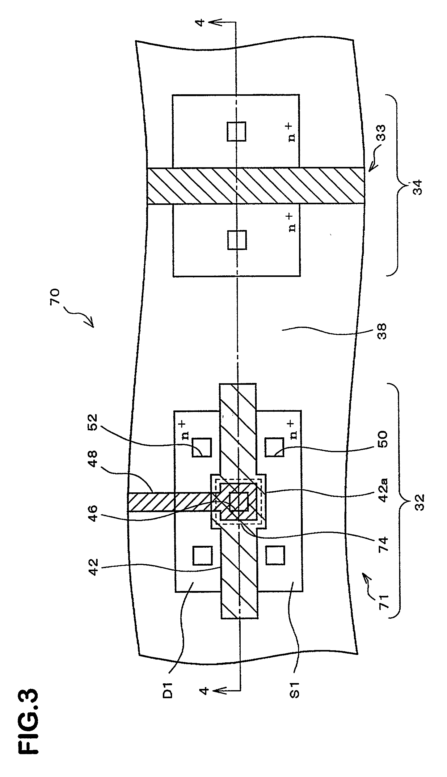
[0039] As shown in FIG. 1, the semiconductor device 30 comprises the transistor 31 and a transistor 33. The transistor 31 is an N channel MOS type field effect transistor which controls the current flowing between source S1 and drain D1 according to the voltage applied to a gate electrode 42 which will be described later. The transistor 33 is also a MOS type field effect transistor. In this embodiment, both transistors are low withstand voltage transistors.

[0040] As shown in FIG. 2, the transistor 31 is formed in a component forming region 32, and the transistor 33 is formed in another component forming region 34. The component forming region 32 and the component forming region 34 are separat...


PUM


Abstract

Provides a semiconductor device that can separate components easily. Gate electrode 42 is formed only within component forming region 32, and gate electrode 42 and aluminum wiring 48 are connected in component forming region 32. Therefore, there is almost no inversion of the surface of the semiconductor substrate 36 that is under field oxide film 38 due to the voltage of the concerned connection area and gate electrode 42. Also, there is interlayer film 44 between aluminum wiring 48 and field oxide film 38, so there is almost no inversion of the surface of the semiconductor substrate 36 that is under field oxide film 38 due to the voltage of aluminum wiring 48. Therefore, it is possible to separate components without increasing overall length L1 of field oxide film 38, increasing the film thickness of field oxide film 38, or increasing the concentration of channel stop ions implanted into the surface of the semiconductor substrate 36 that is under field oxide film 38.

Description

[0001] The entire disclosure of Japanese Patent Application No. Hei 10-14352 filed on Jan. 27, 1998 including specification, claims, drawings and summary are incorporated herein by reference in its entirety.[0002] 1. Field of the Invention[0003] The present invention relates to a semiconductor device, and more particularly to a technique for improving the component separating function of a semiconductor device.[0004] 2. Description of the Related Art[0005] MOS type field effect transistors (Metal Oxide Semiconductor Field Effect Transistor) are known as semiconductor components. FIG. 8 is a conceptual figure of a flat structure of a semiconductor device comprising conventional MOS type field effect transistors (referred to at times hereafter simply as "transistor"). FIG. 9 shows cross-section 9-9 of FIG. 8.[0006] As shown in FIG. 9, a transistor 12 is formed within this semiconductor device. The transistor 12 comprises a channel forming region CH which is sandwiched between source S...

Claims


Application Information

Patent Timeline
Patent Type & Authority Applications(United States)
IPC IPC(8): H01L21/768H01L21/8234H01L23/522H01L21/76H01L27/08
CPCH01L21/823475H01L23/522H01L2924/0002H01L2924/00
Inventor SHIMOJI, NORIYUKI
Owner ROHM CO LTD
Why Eureka
Try Eureka