High frequency module
a high-frequency module and module technology, applied in the field of high-frequency modules, can solve the problems of large warpage, adversely affecting the grinding accuracy of the semiconductor substrate, and easy damage of the semiconductor substrate 104/b>, so as to facilitate the grinding process of the first component, improve the shielding performance of the first component and the second component, and reduce the warpage of the semi-finished product after the first sealing resin layer
- Summary
- Abstract
- Description
- Claims
- Application Information
AI Technical Summary
Benefits of technology
Problems solved by technology
Method used
Image
Examples
first embodiment
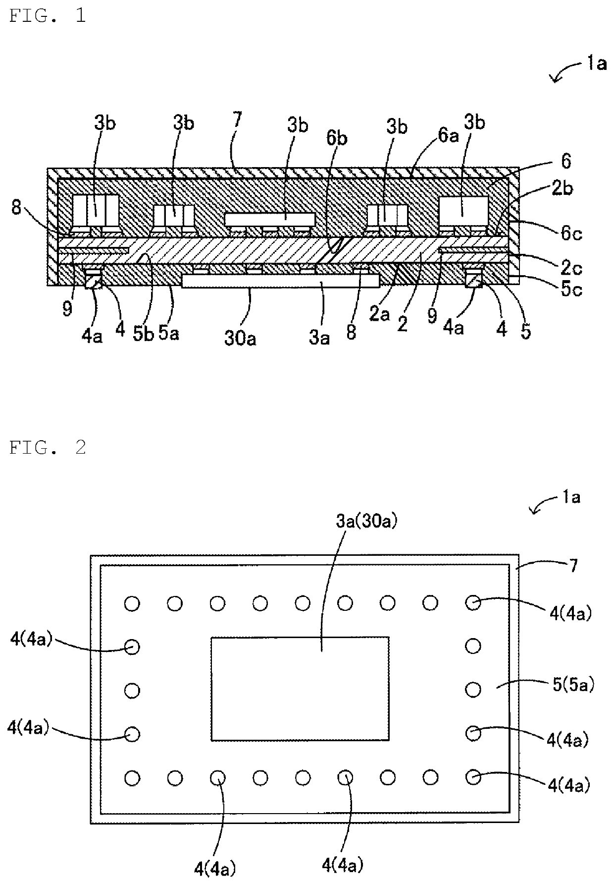
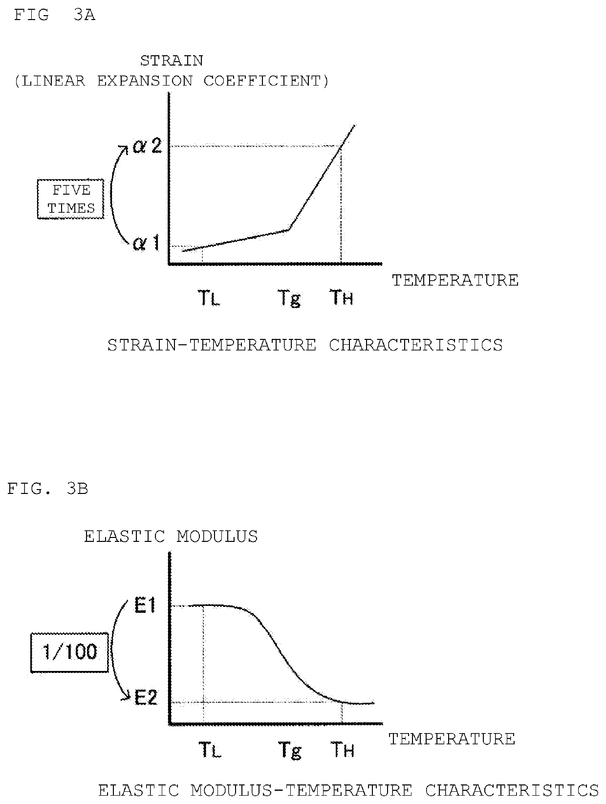
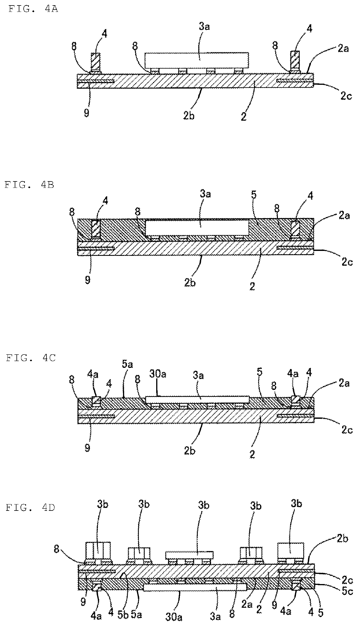
[0026]The configuration of a high frequency module 1a according to a first embodiment of the present disclosure is described with reference to FIGS. 1 to 5C. Note that FIG. 1 is a sectional view of the high frequency module 1a, FIG. 2 is a plan view showing a lower surface 5a of a first sealing resin layer 5 of the high frequency module 1a, FIGS. 3A and 3B are graphs showing relationships between a glass transition temperature, and a linear expansion coefficient and an elastic modulus, and FIGS. 4A to 4D and 5A to 5C are views showing a manufacturing process of the high frequency module 1a.
[0027]As shown in FIGS. 1 and 2, the high frequency module 1a according to this embodiment includes a wiring board 2, a first component 3a and a plurality of connection terminals 4 mounted on a lower surface 2a of the wiring board 2, a first sealing resin layer 5 that seals the first component 3a and the connection terminals 4, a plurality of second components 3b mounted on an upper surface 2b of...
second embodiment
[0047]A high frequency module 1b according to a second embodiment of the present disclosure is described with reference to FIGS. 6 and 7. FIG. 6 is a cross-sectional view of the high frequency module 1b, and FIG. 7 is a plan view showing a lower surface 5a of a first sealing resin layer 5 of the high frequency module 1b.
[0048]The high frequency module 1b according to this embodiment is different from the high frequency module 1a of the first embodiment described with reference to FIGS. 1 and 2 in that, as shown in FIGS. 6 and 7, a plurality of first components 3a are mounted on a lower surface 2a of a wiring board 2 and connection terminals 4 are arranged between the adjacent first components 3a. Other configurations are the same as those of the high frequency module 1a according to the first embodiment, and therefore, the same reference numerals are given and the descriptions thereof are omitted.
[0049]In this embodiment, the two first components 3a are mounted on the lower surface...
third embodiment
[0051]A high frequency module 1c according to a third embodiment of the present disclosure is described with reference to FIGS. 8 and 9. FIG. 8 is a sectional view of the high frequency module 1c, and FIG. 9 is a plan view showing a lower surface 5a of a first sealing resin layer 5 of the high frequency module 1c.
[0052]The high frequency module 1c according to this embodiment is different from the high frequency module 1a of the first embodiment described with reference to FIGS. 1 and 2 in that, as shown in FIGS. 8 and 9, a plurality of connection terminals 40 for external connection are formed as bumps. Other configurations are the same as those of the high frequency module 1a according to the first embodiment, and therefore, the same reference numerals are given and the descriptions thereof are omitted.
[0053]In this embodiment, each of the connection terminals 40 is formed as a bump such as a solder bump or a gold bump on the mounting electrode 8. The connection terminals 40 are ...
PUM
| Property | Measurement | Unit |
|---|---|---|
| glass transition temperature | aaaaa | aaaaa |
| elastic modulus | aaaaa | aaaaa |
| height | aaaaa | aaaaa |
Abstract
Description
Claims
Application Information
 - R&D
- Intellectual Property
- Life Sciences
- Materials
- Tech Scout
- Unparalleled Data Quality
- Higher Quality Content
- 60% Fewer Hallucinations
Browse by: Latest US Patents, China's latest patents, Technical Efficacy Thesaurus, Application Domain, Technology Topic, Popular Technical Reports.
© 2025 PatSnap. All rights reserved.Legal|Privacy policy|Modern Slavery Act Transparency Statement|Sitemap|About US| Contact US: help@patsnap.com


