Method of debonding work-carrier pair with thin devices

a work-carrier and thin-film technology, applied in semiconductor devices, chemistry apparatus and processes, lamination ancillary operations, etc., can solve the problems of high stress on the adhesive and the device wafer, high risk of localized device wafer damage, and debonding of the device wafer from the carrier, so as to improve process efficiency and simplify the procedure , the effect of high wafer throughpu

Active Publication Date: 2021-11-16
CHENGDU ESWIN SYST IC CO LTD
View PDF20 Cites 0 Cited by
  • Summary
  • Abstract
  • Description
  • Claims
  • Application Information

AI Technical Summary

Benefits of technology

[0007]The embodiments of present invention provide effective solutions to problems existing in the mechanical and laser bonding methodologies. The embodiments of the present invention can enhance the process efficiency, simplify the procedure, provide high wafer throughput, and reduce or eliminate the defects such as device wafer breakage and internal device damage.
[0012]In one embodiment, a method of manufacturing a semiconductor device includes: providing a first substrate bonded to a second substrate having an adhesive material therebetween, where the first substrate includes at least one integrated circuit disposed thereon; applying a mechanical force to the at least one of the first substrate and the second substrate in a substantially vertical orientation; and concomitant to the applying step, actuating an external device into direct physical contact with the adhesive layer along a substantially horizontal orientation to facilitate separation of the first substrate from the second substrate. In another embodiment, the method further includes: exposing the first substrate and the second substrate to a chemical solvent further operable to dissolving the adhesive material.
[0014]In one embodiment, a method of manufacturing a semiconductor device includes: providing a first substrate bonded to a second substrate having an adhesive material therebetween, where the first substrate includes at least one integrated circuit disposed thereon; applying an electromagnetic force to the at least one of the first substrate, the second substrate, and the adhesive layer; and concomitant to the applying step, actuating an external device into direct physical contact with the adhesive layer along a substantially horizontal orientation to facilitate separation of the first substrate from the second substrate. In another embodiment, the method further includes: exposing the first substrate and the second substrate to a chemical solvent further operable to dissolving the adhesive material.

Problems solved by technology

This means the release layer will lose adhesion to the carrier once irradiated with a laser beam, thus, resulting in the debonding of device wafer from the carrier.
In mechanical debonding, the adhesive peeling action puts high stress on the adhesive and device wafer and has high risk of localized device wafer damage due to high stress.
With laser debonding method the laser can damage the adhesive and device wafer due to laser misfocus or nonuniformity in the release layer.
Both mechanical and laser debonding could still have residual adhesive remaining and result in incomplete debonding or thinned wafer damage due to local high stress.
All these factors make the mechanical and laser bonding unreliable during high volume production.

Method used


Image

  • Method of debonding work-carrier pair with thin devices
  • Method of debonding work-carrier pair with thin devices
  • Method of debonding work-carrier pair with thin devices

Examples


Embodiment Construction

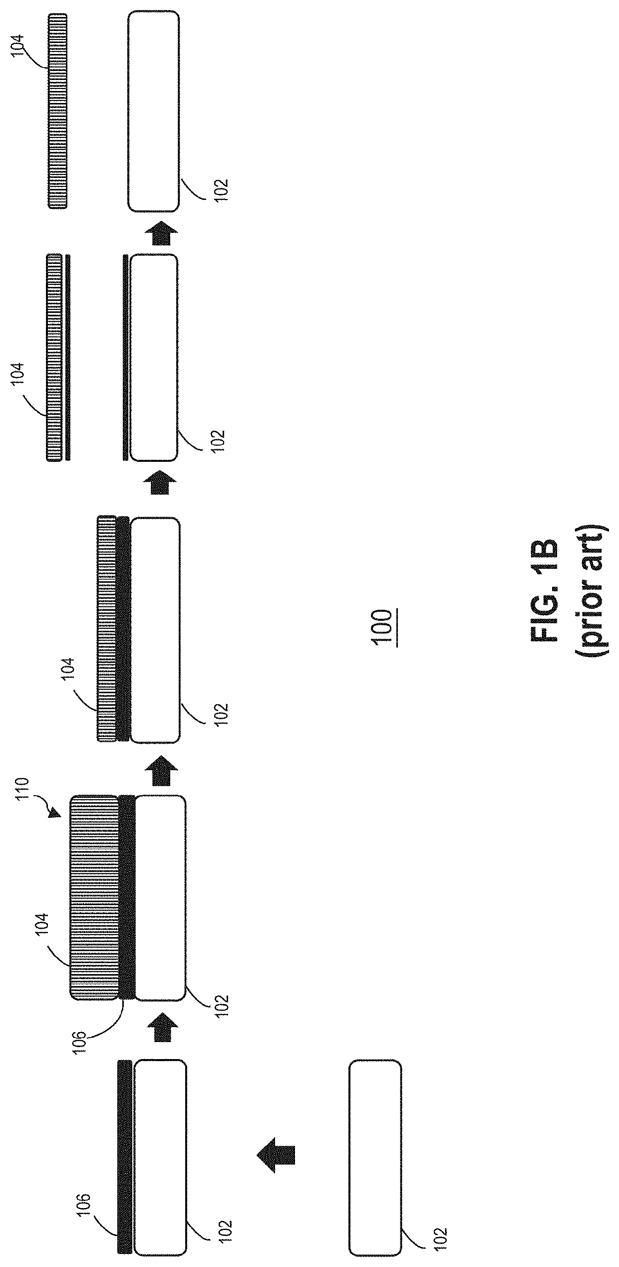
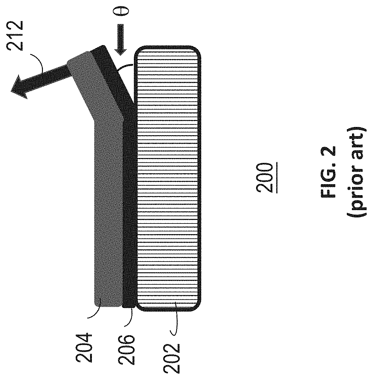
[0029]Disclosed are methods of separating a temporary adhesive bonded carrier-workpiece pair with the use of a thin subject in association with laser debonding or mechanical debonding. This method can be used for processing various workpieces of: different shapes, e.g., round, rectangle, and square, among others; different materials, e.g., silicon, gallium arsenide, sapphire, glass, and metal, among others; different thicknesses, e.g., thick or thin; and different applications, e.g., optical lens, semiconductors, displays-LCD, and solar, among others. In some embodiments, the methods may be useful for debonding temporarily adhesive bonded semiconductor wafers that are used in wafer level packaging and 3D semiconductor wafer packaging (2.5D / 3D).

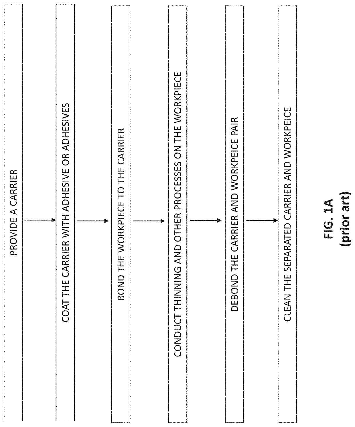
[0030]FIG. 1A is a flow diagram illustrating the steps of prior art temporary wafer bonding, processing, and debonding. As shown, a carrier can be provided, the carrier being coated with an adhesive material, and bonded to a workpiece. Additio...


PUM

PropertyMeasurementUnit
thicknessaaaaaaaaaa
thicknessaaaaaaaaaa
thicknessaaaaaaaaaa

Abstract

Disclosed is a thin subject assisted debonding method for separating temporarily bonded workpiece-carrier pair. The thin subject can be a thin wire, or thin filament, or thin blade. The thin subject can be applied between the workpiece and carrier pair in association with laser debonding or mechanical debonding to provide well controlled and targeted wedging function to the delaminating temporary adhesive and its adjacent substrate to which it is separating from. The workpiece can be a semiconductor wafer that has been thinned and processed, and the carrier can be a semiconductor non-device wafer or any other rigid substrate such as a glass wafer or panel. The application of a thin subject between the workpiece and carrier during debonding provides the advantage of high throughput and low defect rate.

Description

RELATED APPLICATION[0001]The present application claims priority to U.S. Provisional Application No. 62 / 645,184 filed Mar. 20, 2018, entitled “Thin Subject Assisted Debonding Method for Separating Temporary Adhesive Bonded Workpiece-Carrier” which is incorporated herein by reference in its entirety.FIELD OF THE INVENTION[0002]The present disclosure relates generally to electronic devices and, more particularly, to methods of packaging semiconductor devices.BACKGROUND[0003]In many applications, a workpiece needs to be thinned or processed with the support of a carrier to make the workpiece mechanically stable. The workpiece can be temporarily bonded to a support carrier using adhesives. At end of the application, the workpiece needs to be removed or debonded from the carrier, and cleaned of any residual adhesives. Widespread applications of smartphones, tablets, and portable consumer electronics are driving semiconductor packaging towards thinner, smaller and more integrated directio...

Claims


Application Information

Patent Timeline
Patent Type & Authority Patents(United States)
IPC IPC(8): B32B43/00H01L21/683B32B38/10
CPCH01L21/6835B32B38/10B32B43/006H01L2221/68381Y10T156/1111Y10T156/1158Y10T156/1184Y10T156/1917Y10T156/1967H01L2221/68318H01L2221/68327H01L2221/6834H01L2221/68386
Inventor ZHANG, CHUNBINZHOU, XIAOTIAN
Owner CHENGDU ESWIN SYST IC CO LTD
Why Eureka
Try Eureka