Sequenced pulse reverse waveform surface finishing of additively manufactured parts
a reverse waveform and electrochemical technology, applied in the direction of additive manufacturing, process efficiency improvement, electrolysis components, etc., can solve the problems of inacceptable high surface porosity of parts made from 3-d/am processes, and achieve the effect of reducing surface roughness, surface roughness reduction, and surface roughness reduction
- Summary
- Abstract
- Description
- Claims
- Application Information
AI Technical Summary
Benefits of technology
Problems solved by technology
Method used
Image
Examples
example 1
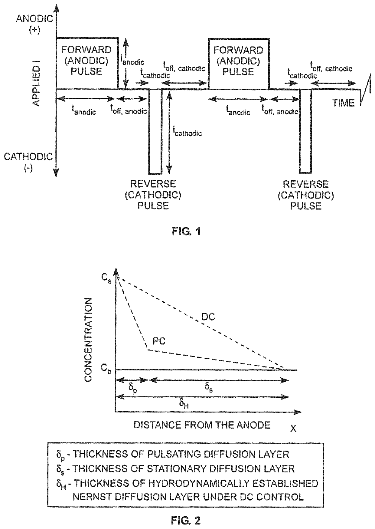
[0048]In this example, two waveforms were applied for electrofinishing of coupons of HASTELLOY® X. The parameters of the waveforms are presented in TABLE I. The initial surface roughnesses of the coupons as measured by Ra was approximately 10 μm (390 μin). After processing to a desired final surface finish of approximately 2 μm (80 μin), both Waveform 1 and Waveform 2 removed approximately 140 μm (5,500 μin) of material as shown in FIG. 5. The time for processing with Waveform 1 was 7 min and for Waveform 2 was 4 min. As noted from FIG. 5, Waveform 1 exhibited a large ΔRa / Δmaterial during the surface finish range of 10 μm (390 μin) to 6 μm (240 μin) Ra. As noted from FIG. 5, Waveform 2 exhibited a large ΔRa / Δmaterial during the surface finish range of 6 μm (240 μin) to 2 μm (80 μin) Ra.
[0049]
TABLE 1Vanodictanodictanodic, offVcathodictcathodictcathodic, off(V)(msec)(msec)(V)(msec)(msec)Waveform 1400.10300.10Waveform 2400.70200.50
[0050]In TABLE II presents the results of processing wi...
example 2
[0052]In this example, two waveform sequences were applied with different allotted times for electrofinishing of coupons of Ti6Al4V. The parameters of the waveforms used in the sequences are presented in TABLE III. The beginning surface roughnesses of the coupons as measured by Ra was approximately 7 μm (275 μin). The waveform sequences consisted of Waveform 3 followed by Waveform 4 followed by Waveform 5. The data from Trial A are presented in TABLE IV. With the waveform sequence in Trial A, the initial surface roughness was 7.0 / 276 (μm / μin) Ra and the final surface roughness was 1.98 / 78 (μm / μin) Re with material removed of 664 / 26141 (μm / μin).
[0053]
TABLE IIIVanodictanodictanodic, offVcathodictcathodictcathodic, off(V)(msec)(msec)(V)(msec)(msec)Waveform 360.50120.70Waveform 460.30120.60Waveform 560.20120.40
[0054]
TABLE IVTRIAL ATotalProcessingInitialFinalMaterialMaterialTimeRaRaRemovedRemoved(hr)(μm / μin)(μm / μin)(μm / μin)(μm / μin)Waveform47.0 / 2764.9 / 193 266 / 104723PlusWaveform24.9 / 193NAN...
example 3
[IN718]
[0057]Electropolish of sample B320_2_60 was processed with the waveforms developed for EMB HIP IN 718 coupon B315_2_60 using 10% (w / w) H2SO4 electrolyte. For this coupon, Faraday varied the applied time for each of the five waveforms to enable development of an appropriately timed waveform sequence. As such, Faraday began polishing the SLM HIP IN 718 surfaces using the conditions of waveform N, pulling the sample every two minutes to evaluate the surface roughness, and mass loss. The data collected for this sample is presented in TABLE VI. FIGS. 6 and 7 show the calculated etch depth with time and change in Ra with time, respectively. The 3D images collected from the Nanovea optical profilometer are given for this sample in FIG. 8, including initial surface and surface after processing with the waveforms outlined in TABLE VII, and sample photographs showing the polishing evolution is given in FIG. 9.
[0058]
TABLE VIVanodictanodictanodic, offVcathodictcathodictcathodic, off(V)(m...
PUM
| Property | Measurement | Unit |
|---|---|---|
| cathodic voltages | aaaaa | aaaaa |
| cathodic voltages | aaaaa | aaaaa |
| cathodic voltages | aaaaa | aaaaa |
Abstract
Description
Claims
Application Information
 - Generate Ideas
- Intellectual Property
- Life Sciences
- Materials
- Tech Scout
- Unparalleled Data Quality
- Higher Quality Content
- 60% Fewer Hallucinations
Browse by: Latest US Patents, China's latest patents, Technical Efficacy Thesaurus, Application Domain, Technology Topic, Popular Technical Reports.
© 2025 PatSnap. All rights reserved.Legal|Privacy policy|Modern Slavery Act Transparency Statement|Sitemap|About US| Contact US: help@patsnap.com


