
Silicon carbide semiconductor device and method of manufacturing a silicon carbide semiconductor device

a semiconductor device and silicon carbide technology, applied in semiconductor devices, diodes, electrical devices, etc., can solve the problems of low current density of power mosfets, high possibility of exceeding the material limit of silicon, and difficult to adapt for larg

Active Publication Date: 2021-06-15
FUJI ELECTRIC CO LTD
View PDF6 Cites 1 Cited by
  • Summary
  • Abstract
  • Description
  • Claims
  • Application Information

AI Technical Summary

Benefits of technology

[0016]Further, there is a technique of reducing minority carriers within a boundary layer where at the time of epitaxial growth or after epitaxial growth, by using any one of transition metal doping, or an externally generated specific defect or a specific internal growth defect by an electron or a proton irradiation technique and introducing a lifetime killer (for example, refer to Japanese Patent No. 4939777). Further, there is a technique of forming a crystal defect by implanting at least, helium (He), noble gas, platinum (Pt), vanadium (V), group 4 ions, etc. into a silicon carbide semiconductor substrate (for example, refer to U.S. Patent Application Publication No. 2017 / 0012102).

Problems solved by technology

On the other hand, power MOSFETs have low current density compared to bipolar transistors and IGBTs, and are difficult to adapt for large current but can be switched at high speeds up to about several MHz.
Further, silicon carbide has a critical electric field strength that is ten times that of silicon or greater, and has a high possibility of exceeding the material limit of silicon.
When such operation continues, the stacking defect cumulatively expands, whereby loss that occurs in the inverter circuit increases over time and the amount of heat generated increases, causing device failure.

Method used


Image

  • Silicon carbide semiconductor device and method of manufacturing a silicon carbide semiconductor device
  • Silicon carbide semiconductor device and method of manufacturing a silicon carbide semiconductor device
  • Silicon carbide semiconductor device and method of manufacturing a silicon carbide semiconductor device

Examples


first embodiment

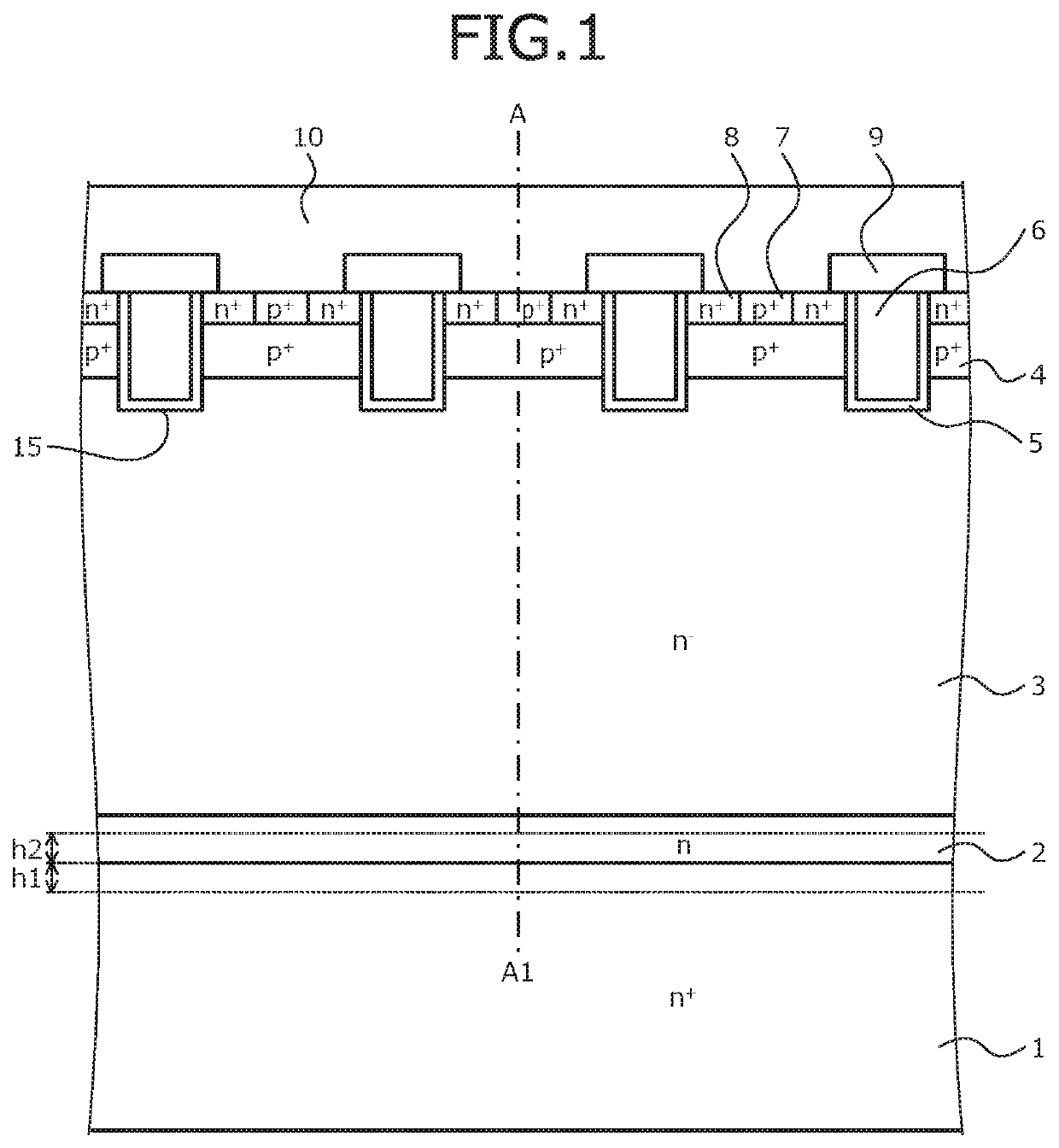
[0070]In the silicon carbide semiconductor device of the first embodiment, protons are implanted as a lifetime killer near an interface of the n+-type silicon carbide semiconductor substrate 1 and the n-type boundary layer 2. The protons are lifetime killers and may reduce the hole density at the interface of the n+-type silicon carbide semiconductor substrate 1 and the n-type boundary layer 2 by 100 times or more. As a result, hole and electron recombination may be reduced and the growth of crystal defects may be suppressed.

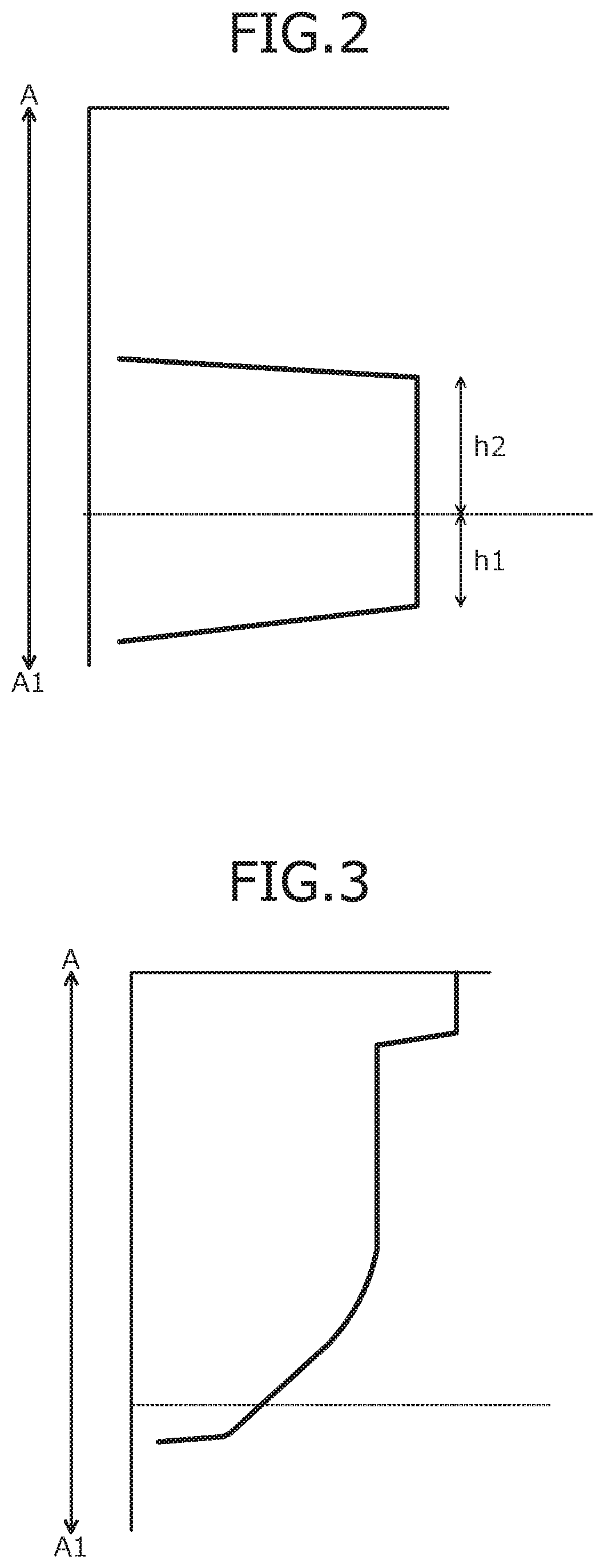
[0071]FIG. 2 is a graph of proton concentration of the silicon carbide semiconductor device according to the first embodiment. FIG. 2 depicts proton concentration of a part along line A-A′ in FIG. 1. In FIG. 2, a vertical axis indicates depth from the surface of the p+-type contact region 7 and a horizontal axis indicates proton concentration. Further, a dotted line parallel to the horizontal axis indicates the interface of the n+-type silicon carbide semiconduc...

second embodiment

[0093]As depicted in FIG. 9, protons are implanted in a region of the n−-type drift layer 3, the region spanning a distance h3 from a surface of the n−-type drift layer 3 facing toward the n-type boundary layer 2. The distance h3 is, for example, the film thickness of the n−-type drift layer 3. FIG. 10 is a graph of proton concentration of the silicon carbide semiconductor device according to the FIG. 10 depicts the proton concentration of a part along line A-A′ in FIG. 9. In FIG. 10, a vertical axis indicates depth from a surface of the p+-type contact region 7 and a horizontal axis indicates proton concentration. Further, a dotted line parallel to the horizontal axis indicates the interface of the n+-type silicon carbide semiconductor substrate 1 and the n-type boundary layer 2.

[0094]As depicted in FIG. 10, a concentration of the protons of the n−-type drift layer 3 is lower than a concentration of the protons implanted in the n+-type silicon carbide semiconductor substrate 1 and...

fifth embodiment

[0112]In the silicon carbide semiconductor device of the fifth embodiment, protons are implanted as a lifetime killer near an interface of the p-type silicon carbide semiconductor substrate 16 and the n-type boundary layer 2, and near an interface of the n−-type drift layer 3 and the p+-type base region 4. The IGBT performs bipolar operation and therefore, crystal defects also grow from the interface of the n−-type drift layer 3 and the p+-type base region 4, and thus, protons are also implanted near the interface of the n−-type drift layer 3 and the p+-type base region 4.

[0113]The protons become a lifetime killer, enabling the hole density of the interface of the p-type silicon carbide semiconductor substrate 16 and the n-type boundary layer 2 and the hole density of the interface of the n−-type drift layer 3 and the p+-type base region 4 to be reduced. As a result, hole and electron recombination is reduced, enabling the growth of crystal defects to be suppressed.

[0114]FIG. 21 is ...


PUM

PropertyMeasurementUnit
thicknessaaaaaaaaaa
thicknessaaaaaaaaaa
thicknessaaaaaaaaaa

Abstract

A silicon carbide semiconductor device includes a semiconductor substrate and a first semiconductor layer of the first conductivity type; a second semiconductor layer of a second conductivity type; a first semiconductor region of the first conductivity type; a gate electrode provided opposing at least a surface of the second semiconductor layer between the first semiconductor region and the first semiconductor layer, across a gate insulating film; and a first electrode provided on surfaces of the first semiconductor region and the second semiconductor layer. Protons are implanted in a first region of the semiconductor substrate, spanning at least 2 μm from a surface of the semiconductor substrate facing toward the first semiconductor layer; and in a second region of the first semiconductor layer, spanning at least 3 μm from a surface of the first semiconductor layer facing toward the semiconductor substrate. The protons having a concentration in a range from 1×10¹³ / cm3 to 1×10¹⁵ / cm3.

Description

CROSS REFERENCE TO RELATED APPLICATIONS[0001]This application is based upon and claims the benefit of priority of the prior Japanese Patent Application No. 2017-228293, filed on Nov. 28, 2017, the entire contents of which are incorporated herein by reference.BACKGROUND1. Field[0002]Embodiments of the invention relate to a silicon carbide semiconductor device and a method of manufacturing a silicon carbide semiconductor device.2. Description of Related Art[0003]Silicon (Si) is used as a material for power semiconductor devices that control high voltage and / or large current. There are several types of power semiconductor devices such as bipolar transistors, insulated gate bipolar transistors (IGBTs), and metal oxide semiconductor field effect transistors (MOSFETs). These devices are selectively used according to an intended purpose.[0004]For example, bipolar transistors and IGBTs have high current density compared to MOSFETs, and can be adapted for large current but cannot be switched...

Claims


Application Information

Patent Timeline
Patent Type & Authority Patents(United States)
IPC IPC(8): H01L29/08H01L29/78H01L29/16H01L29/66H01L29/739H01L21/04
CPCH01L29/0878H01L21/046H01L29/0821H01L29/1608H01L29/66068H01L29/7397H01L29/7805H01L29/7813H01L29/0834H01L29/66348H01L29/36H01L21/2605H01L21/26506H01L29/32H01L21/221
Inventor FUJIMOTO, TAKUMI
Owner FUJI ELECTRIC CO LTD
Learn More