MTJ device performance by controlling device shape

a technology of mtj device and shape, which is applied in the direction of magnetic field controlled resistors, galvano-magnetic material selection, magnetic bodies, etc., can solve the problems of not using the same methods or producing the same effects, difficult to achieve high tmr (tunneling magneto resistance) values, and significant structure strain, etc., to improve the performance of layered mtj devices, reduce interfacial defect concentration, and improve lattice epitaxy

Active Publication Date: 2021-03-09
TAIWAN SEMICON MFG CO LTD
View PDF8 Cites 1 Cited by
  • Summary
  • Abstract
  • Description
  • Claims
  • Application Information

AI Technical Summary

Benefits of technology

[0006]A first object of the present disclosure is to provide a method of improving the performance of a layered MTJ device by controlling its shape.
[0007]A second object of the present disclosure is to provide such a method that reduces interfacial defect concentrations and lattice mismatches and improves lattice epitaxy, thereby creating a measurable improvement in TMR.
[0008]A third object of the present disclosure is to provide such a method that allows controlling and manipulating the shape of a layered device during its fabrication, in effect customizing its shape.
[0009]A fourth object of the present disclosure is to control the stresses in a TMJ layered film stack or similar device structure by controlling its shape so that the stresses thereby cause crystal defects to migrate towards regions of the structure that can be subsequently removed.
[0010]These objects will be achieved through the design and fabrication of a patterned, layered MTJ device during which its shape is controlled in such a manner that crystal defects such as vacancies, pinholes and dislocations within the stack are moved to an undesirable weak zone which can subsequently be removed. The relatively defect-free remaining portion of the device will have a higher coercivity and improved TMR values. The new device shape will, therefore, reduce the interface defect concentration and improve the interface lattice epitaxy, both results leading to improvement of device performance as, for example, measured by the improved TMR values.

Problems solved by technology

In particular, the strain in the structure can significantly alter the properties of the device, for reasons to be discussed below.
Imperfections in the interfaces make it difficult to achieve high TMR (Tunneling Magneto Resistance) values, which measure the ability of the electrons to successfully tunnel when the proper magnetization conditions are met.
Such imperfections result from lattice mismatches between the ferromagnetic layers and the non-magnetic barrier layer and from defects that occur during crystal growth of materials.
However these attempts do not use the same methods or produce the same effects as will be described herein.

Method used


Image

  • MTJ device performance by controlling device shape
  • MTJ device performance by controlling device shape
  • MTJ device performance by controlling device shape

Examples


Embodiment Construction

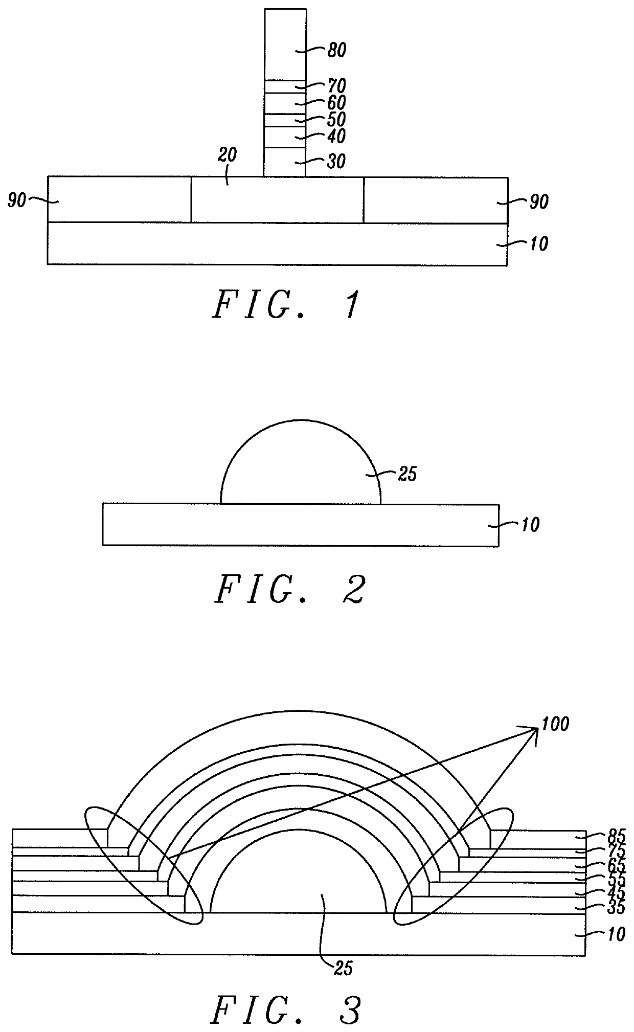
[0021]Referring first to FIG. 1, there is shown a standard patterned MTJ (Magnetic Tunneling Junction) layered device such as is commonly used in a random access memory (RAM) array. Although a specific substrate is not necessary to define the device, for specificity we will consider the device to be formed on a functional substrate, such as a CMOS substrate, that may already include circuitry and conducting vias to access various elements of the devices in a RAM array.

[0022]The device is formed by first providing a CMOS substrate 10 on which to form it. A blanket bottom electrode (BE) 20 is deposited on the CMOS substrate so that it properly contacts the vias in that substrate. There is then deposited on top of the bottom electrode 20, in succession, a series of horizontal layers that will comprise the MTJ stack. Those layers include, a seed layer 30, a pinned magnetic layer 40, a tunnel barrier layer 50, a free magnetic layer 60 and capping layer 70. A hard mask 80 is deposited on ...


PUM

PropertyMeasurementUnit
widthaaaaaaaaaa
widthaaaaaaaaaa
widthaaaaaaaaaa

Abstract

A layered thin film device, such as a MTJ (Magnetic Tunnel Junction) device can be customized in shape by sequentially forming its successive layers over a symmetrically curved electrode. By initially shaping the electrode to have a concave or convex surface, the sequentially formed layers conform to that shape and acquire it and are subject to stresses that cause various crystal defects to migrate away from the axis of symmetry, leaving the region immediately surrounding the axis of symmetry relatively defect free. The resulting stack can then be patterned to leave only the region that is relatively defect free.

Description

BACKGROUND1. Technical Field[0001]This disclosure relates generally to magnetic memory devices, specifically to the effect of the shape of a device on its performance.2. Description of the Related Art[0002]The crystalline property of the structure of a magnetic memory device, specifically that of the ferromagnetic / MgO tunneling barrier interface of a MTJ (magnetic tunneling junction) device, plays a very critical role in the device performance. In particular, the strain in the structure can significantly alter the properties of the device, for reasons to be discussed below.[0003]Magnetic memory devices comprise a stack of layers in which two ferromagnetic layers, typically referred to as a reference layer and a free layer, are separated by a thin, non-magnetic dielectric layer, called a barrier layer. In the classical physics regime, a current of electrons going from one ferromagnetic layer to the other would be unable to pass through the barrier layer, which is non-conducting; but ...

Claims


Application Information

Patent Timeline
Patent Type & Authority Patents(United States)
IPC IPC(8): H01L43/12H01F10/06H01F10/16H01L43/02H01L43/08H01L43/10
CPCH01L43/12H01F10/06H01F10/16H01L43/02H01L43/08H01L43/10H10N50/10H10N50/01H10N50/80H10N50/85
Inventor HAQ, JESMINZHONG, TOMTENG, ZHONGJIANLAM, VINHYANG, YI
Owner TAIWAN SEMICON MFG CO LTD
Why Eureka
Try Eureka