
Complementary magnetic memory cell

a magnetic memory cell and memory cell technology, applied in the field of complementary magnetic memory cells, can solve the problems of high energy waste, low power consumption, and inability to reduce the current required for the magnetic field writing technology, and achieve the effects of reducing read error rates, high read error rates, and overhead additional areas

Active Publication Date: 2021-02-02
BEIHANG UNIV
View PDF6 Cites 0 Cited by
  • Summary
  • Abstract
  • Description
  • Claims
  • Application Information

AI Technical Summary

Benefits of technology

[0005]An object of the present invention is to provide a complementary magnetic memory cell, wherein in view of the drawbacks faced by the conventional MRAM mentioned in the above background, especially the write asymmetry problem of STT-MRAM, the additional area overhead and high read error rate of SOT-MRAM, the present invention adopts a pair of magnetic tunnel junctions with complementary states to store data, reducing read error rates; the device structure and write mechanism are optimized, solving the above-mentioned write asymmetry problem and additional area overhead.

Problems solved by technology

As the feature size of the semiconductor process continues to decrease, the static power consumption caused by the transistor leakage current is increasing in the total power consumption of the integrated circuit, causing serious energy waste.
The more serious problem is that as the device size decreases, the current required for the magnetic field writing technology cannot be reduced, which prohibits development of MRAM with large capacity and low power consumption.
However, the write current of the STT-MRAM directly passes through the ultra-thin barrier layer of the magnetic tunnel junction, which easily causes breakdown and failure of the device, and the power consumption required and delay when writing from the low resistance state to the high resistance state are larger than those of another write case (hereinafter referred to as the write asymmetry problem of spin transfer torque), which is not conducive to the design and optimization of the MRAM circuit.
However, the SOT-MRAM memory cell has three terminals and typically requires two access transistors, causing additional area overhead.
In addition, the ratio of the high and low resistance values of the memory cell is small, which tends to cause an increase in the read error rate.

Method used


Image

  • Complementary magnetic memory cell
  • Complementary magnetic memory cell
  • Complementary magnetic memory cell

Examples


Embodiment Construction

[0084]The substantial features of the present invention are further described with reference to the drawings. The figures are schematic representations in which the thickness of each functional layer or region involved is not the actual size, and the resistance, current and voltage values in the operating mode are also not actual values.

[0085]Detailed exemplary embodiments are disclosed herein, and the specific structural details and functional details are only for the purpose of describing. Embodiments have been shown and described for the purposes of illustrating the functional and structural principles of the present invention and is subject to change without departure from such principles. Therefore, this invention includes all modifications encompassed within the spirit and scope of claims.

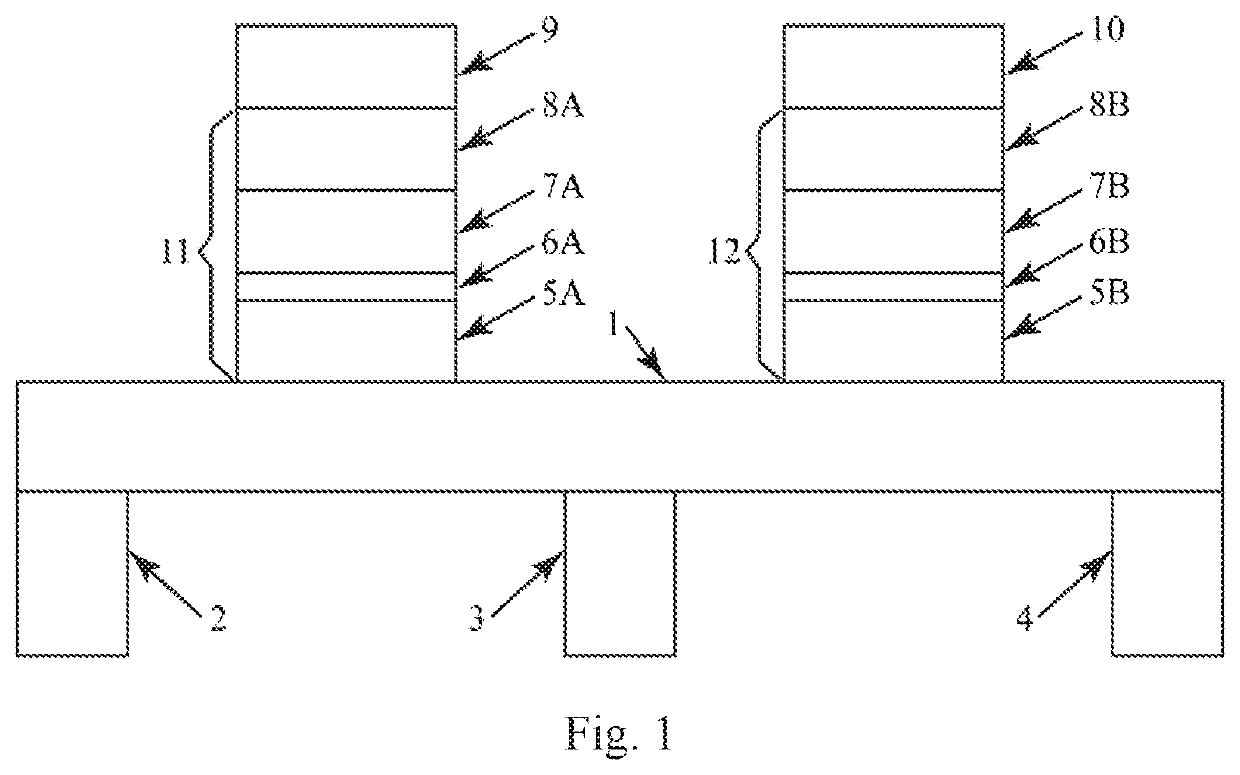
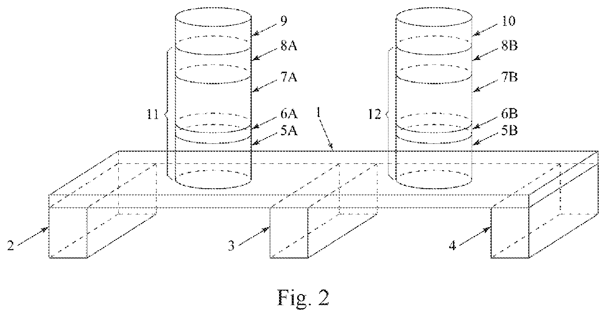
[0086]The present invention provides a complementary magnetic memory cell which can be used for constructing a magnetic random access memory as well as for designing a magnetic logic circuit....


PUM

PropertyMeasurementUnit
thicknessaaaaaaaaaa
aspect ratioaaaaaaaaaa

Abstract

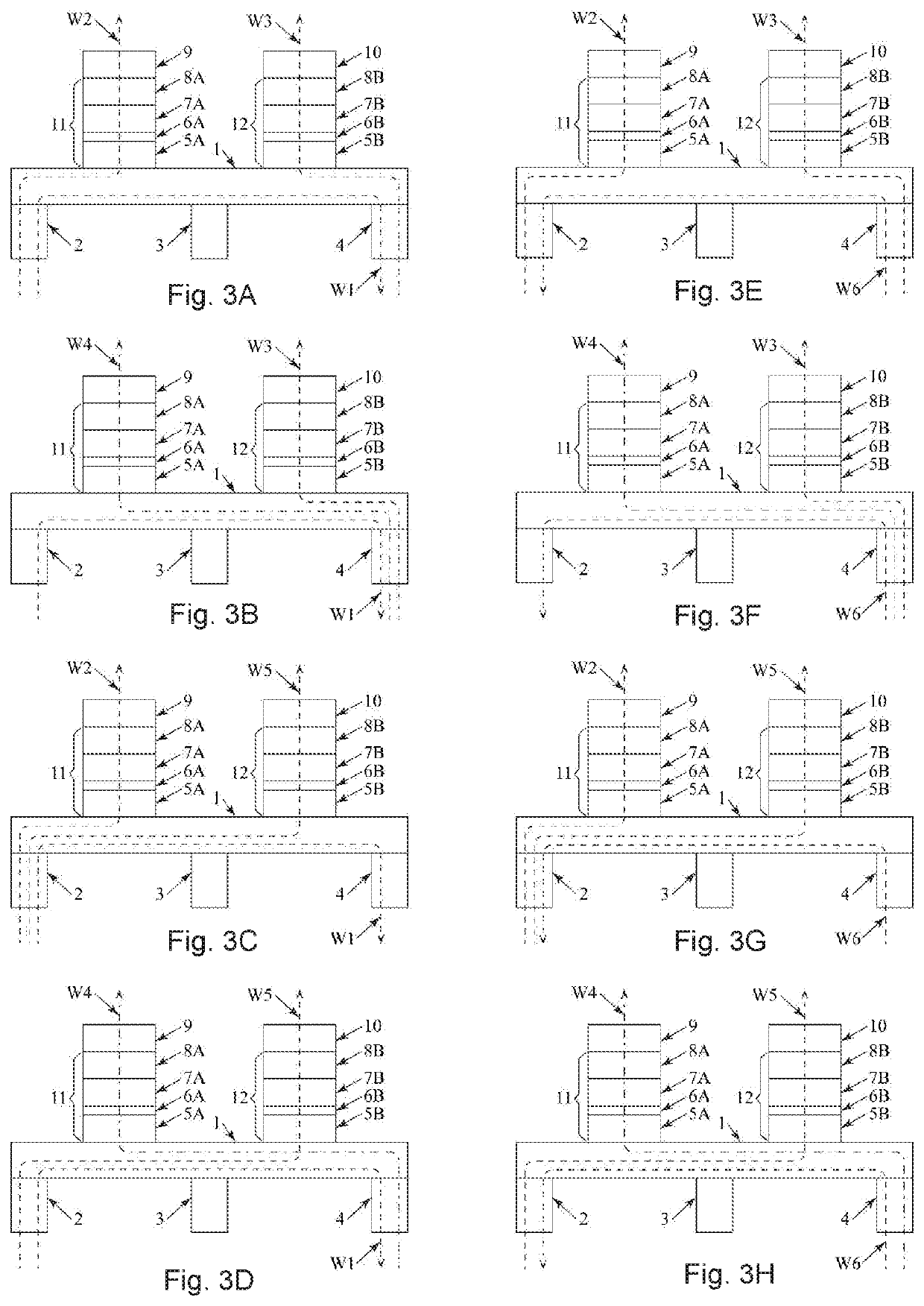
A complementary magnetic memory cell includes: a heavy metal film or an antiferromagnetic film, a first magnetic tunnel junction, a second magnetic tunnel junction, a first electrode, a second electrode, a third electrode, a fourth electrode, and a fifth electrode; wherein the first magnetic tunnel junction and the second magnetic tunnel junction are fabricated above the heavy metal film or the antiferromagnetic film; the first electrode, the second electrode and the third electrode are fabricated under the heavy metal film or the antiferromagnetic film; the fourth electrode is fabricated above the first magnetic tunnel junction, and the fifth electrode is fabricated above the second magnetic tunnel junction; to store one bit of data, the first magnetic tunnel junction and the second magnetic tunnel junction are arranged in a pair of complementary resistance states, wherein one magnetic tunnel junction is set to a high resistance state and the other remains unchanged.

Description

CROSS REFERENCE OF RELATED APPLICATION[0001]The present invention claims priority under 35 U.S.C. 119(a-d) to CN 201810901797.0, filed Aug. 9, 2018.BACKGROUND OF THE PRESENT INVENTIONField of Invention[0002]The present invention relates to a complementary magnetic memory cell, which uses a pair of magnetic tunnel junctions with complementary states to store data, belonging to a field of non-volatile storage and logic technology.Description of Related Arts[0003]As the feature size of the semiconductor process continues to decrease, the static power consumption caused by the transistor leakage current is increasing in the total power consumption of the integrated circuit, causing serious energy waste. Emerging non-volatile memory can save data in the power-off state, which is one of the effective solutions to solve the static power consumption problem of integrated circuits. Among them, a magnetic random access memory (MRAM) based on a magnetic tunnel junction is expected to become a ...

Claims


Application Information

Patent Timeline
Patent Type & Authority Patents(United States)
IPC IPC(8): G11C11/16G11C11/22G11C11/18
CPCG11C11/1673G11C11/161G11C11/1659G11C11/1675G11C11/18G11C11/2275G11C11/1693H10N50/85H10N50/10
Inventor ZHAO, WEISHENGWANG, ZHAOHAODENG, ERYA
Owner BEIHANG UNIV
Learn More