
Methods of filtering reference voltage noise

a reference voltage and noise filtering technology, applied in the field of reference voltage noise filtering, can solve the problems of adversely affecting performance, ctsdms as well as other adcs and dacs are also susceptible to external reference noise, and achieve the effect of reducing gain drift with temperatur

Active Publication Date: 2020-09-01
ANALOG DEVICES INT UNLTD
View PDF4 Cites 2 Cited by
  • Summary
  • Abstract
  • Description
  • Claims
  • Application Information

AI Technical Summary

Benefits of technology

This patent text describes a sample embodiment where a resistor is located on the same semiconductor chip as the converter and a reference gain trimming circuit. The resistor can also be made of the same material type as the converter to reduce changes in the signal caused by temperature. The technical effect of this arrangement is that it can improve the accuracy of the signal conversion and reduce the effects of external factors that may affect the system.

Problems solved by technology

However, in one approach, CTSDMs use a current digital-to-analog converter (DAC) in a feedback path that can suffer from input-dependent reference errors.
Though techniques such as quad-switching have been used to address such errors, CTSDMs as well as other ADCs and DACs are also susceptible to external reference noise.
For example, values of external components such as voltage references may drift with temperature and over time, which adversely impacts performance.

Method used


Image

  • Methods of filtering reference voltage noise
  • Methods of filtering reference voltage noise
  • Methods of filtering reference voltage noise

Examples


Embodiment Construction

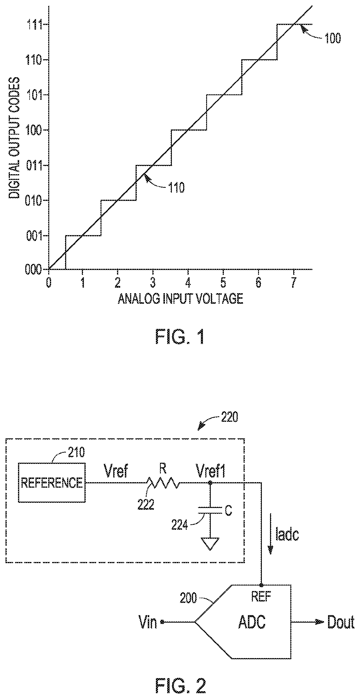
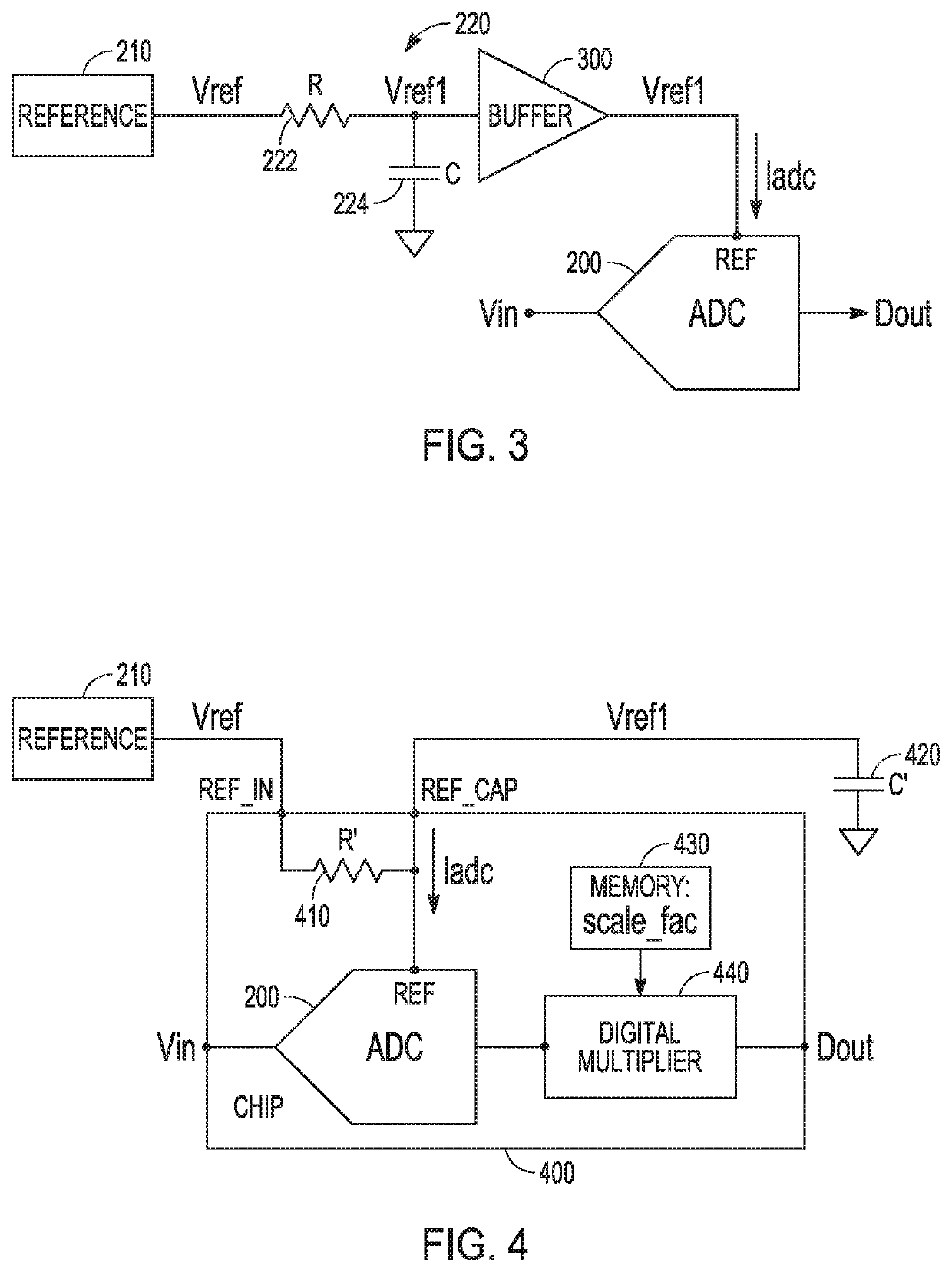
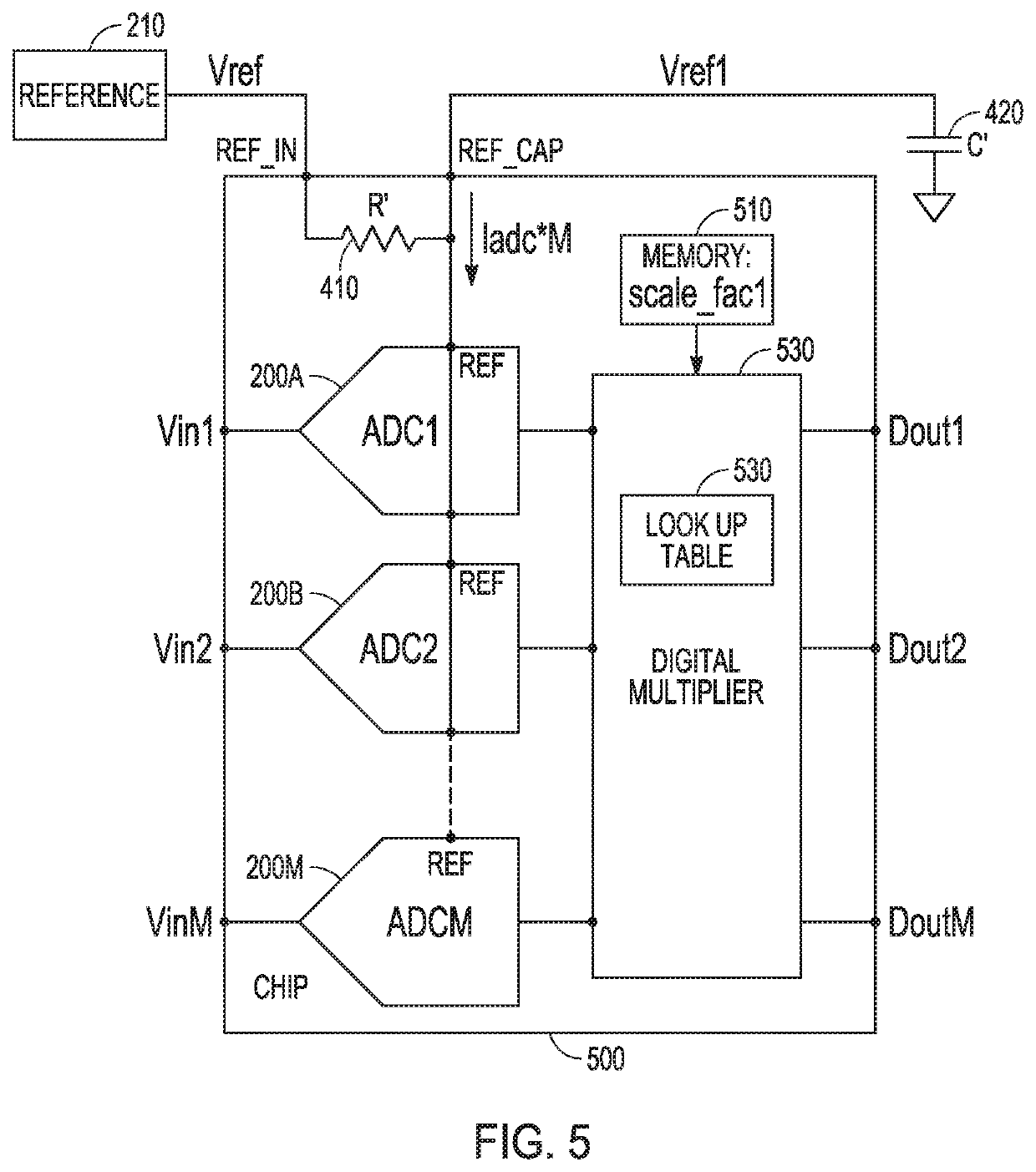
[0021]The following description with respect to FIGS. 1-6 sufficiently illustrates specific embodiments to enable those skilled in the art to practice them. Other embodiments may incorporate structural, logical, process, and other changes. Portions and features of some embodiments may be included in, or substituted for, those of other embodiments. Embodiments set forth in the claims encompass all available equivalents of those claims. The example embodiments are presented for illustrative purposes only and are not intended to be restrictive or limiting on the scope of the disclosure or the claims presented herein.

[0022]The following disclosure will describe a voltage reference noise filter for any circuit like an analog-to-digital converter (ADC) or digital-to-analog converter (DAC) where the reference load current is a constant load and the circuit uses external components that have values that may vary with temperature, over time, and the like. While the implementation illustrated...


PUM


Abstract

A voltage reference noise filter is provided that substantially eliminates noise with minimal external components for any circuit where the reference load current is a constant load and the circuit uses external components that have values that may vary with temperature, over time, and the like. The drift on an output of a voltage reference due to variation of resistor of the external filter is mitigated by moving the external resistor onto the chip containing the circuit. The voltage drop across the resistor is digitally compensated by a scaling factor determined during calibration. When more than one converter is provided on the chip, a further adjustment to the outputs of the converters is made based on the number of converters powered on or off. Also, error in output of converters due to mismatch among the converters is digitally compensated by a further scaling factor.

Description

FIELD OF THE DISCLOSURE[0001]This document relates to an apparatus to filter external reference noise for any circuit having a constant reference load current and, in particular, to a reference voltage noise filter for analog-to-digital or digital-to-analog converters where the reference load current is a constant load.BACKGROUND[0002]Analog-to-digital converters (ADCs) and, in particular, continuous-time sigma-delta modulators (CTSDMs) are gaining popularity due to power-efficient operation well-suited for high-speed, high-performance systems. In a CTSDM, typically an input analog signal that varies over time is converted into a digital stream that represents the input with high fidelity in the frequency band of interest. This digital stream then goes through digital post-processing (typically decimation) to provide the final digital code stream which represents the analog input signal in the digital domain with high fidelity.[0003]However, in one approach, CTSDMs use a current dig...

Claims


Application Information

Patent Timeline
Patent Type & Authority Patents(United States)
IPC IPC(8): H03M1/34H03M1/36G05F1/46H03M1/10
CPCG05F1/468H03M1/365H03M1/1014H03M1/54H03M1/123H03M1/0845
Inventor NITTALA, VENKATA ARUNA SRIKANTHKAWLE, ABHILASHARAJENDRAN, RAJASEKAR
Owner ANALOG DEVICES INT UNLTD
Learn More