


Quick Research
Generate reliable direction feasibility study reports for your R&D in just a few steps.

Technical Q&A
Discover and master advanced knowledge NOW. Basics, ideas, possibilities, all at once.

Find Solutions
As an expert in R&D theories, this can generate solutions to your technical problems instantly.

Evaluate Feasibility
Analyze your overall solution with one click, know your potential R&D risks in advance.

Monitor Landscape
Get weekly tech updates, stay abreast of the latest tech innovations and key insights.
Method for growing high resistant GaN film
A thin-film, high-resistance technology, applied in the manufacture of electrical components, circuits, semiconductor/solid-state devices, etc., can solve problems such as system pollution and affect device performance, and achieve high surface flatness, simple and easy methods, and process compatibility. Effect
- Summary
- Abstract
- Description
- Claims
- Application Information
AI Technical Summary
Problems solved by technology
Method used
Image

Examples
Embodiment 1
[0019] Embodiment 1, growing GaN film
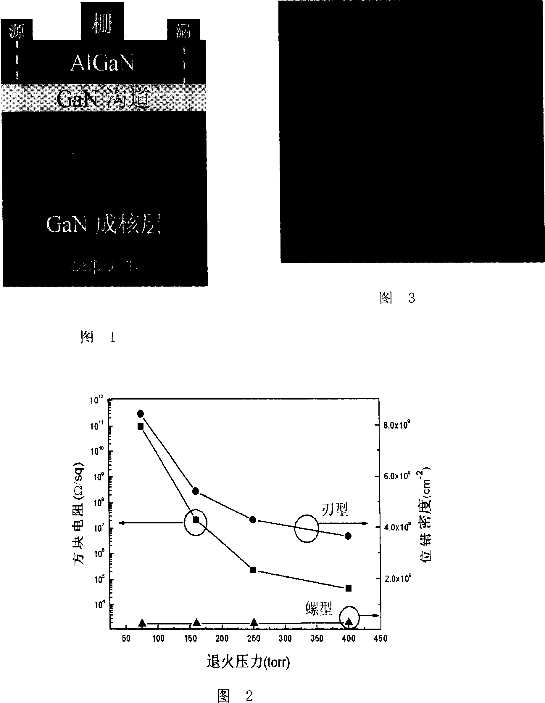
[0020] 1) Metal-organic chemical vapor deposition (MOCVD) equipment is used, the substrate is a sapphire substrate with (0001) surface, and H 2 , the reaction chamber pressure is 300torr, heated at 1100°C for 15min to clean the substrate;
[0021] 2) Cool down to about 550°C, feed trimethylgallium and ammonia gas, H 2 as a carrier gas. The reaction chamber pressure is 300torr, and the buffer layer is grown at a growth rate of 300nm per hour, with a thickness of 25nm;
[0022] 3) Stop feeding trimethylgallium, continue to feed ammonia gas, reduce the reaction chamber pressure to 75torr, 160torr, 250torr, 400torr (according to the data in Figure 2) in 60 seconds, and raise the temperature to 1070°C, keep 60 seconds;
[0023] 4) Introduce trimethylgallium, and epitaxially grow a GaN film at a growth rate of 2000 nm per hour at 1070° C., with a thickness of 2000 nm.
[0024] There are two types of dislocations in GaN films grown by MOCV...
PUM
| Property | Measurement | Unit |
|---|---|---|
| thickness | aaaaa | aaaaa |
Abstract
Description
Claims
Application Information
 - R&D Engineer
- R&D Manager
- IP Professional
- Industry Leading Data Capabilities
- Powerful AI technology
- Patent DNA Extraction
Browse by: Latest US Patents, China's latest patents, Technical Efficacy Thesaurus, Application Domain, Technology Topic, Popular Technical Reports.
© 2024 PatSnap. All rights reserved.Legal|Privacy policy|Modern Slavery Act Transparency Statement|Sitemap|About US| Contact US: help@patsnap.com