
Method for preventing clearance generation between different materials in semiconductor device

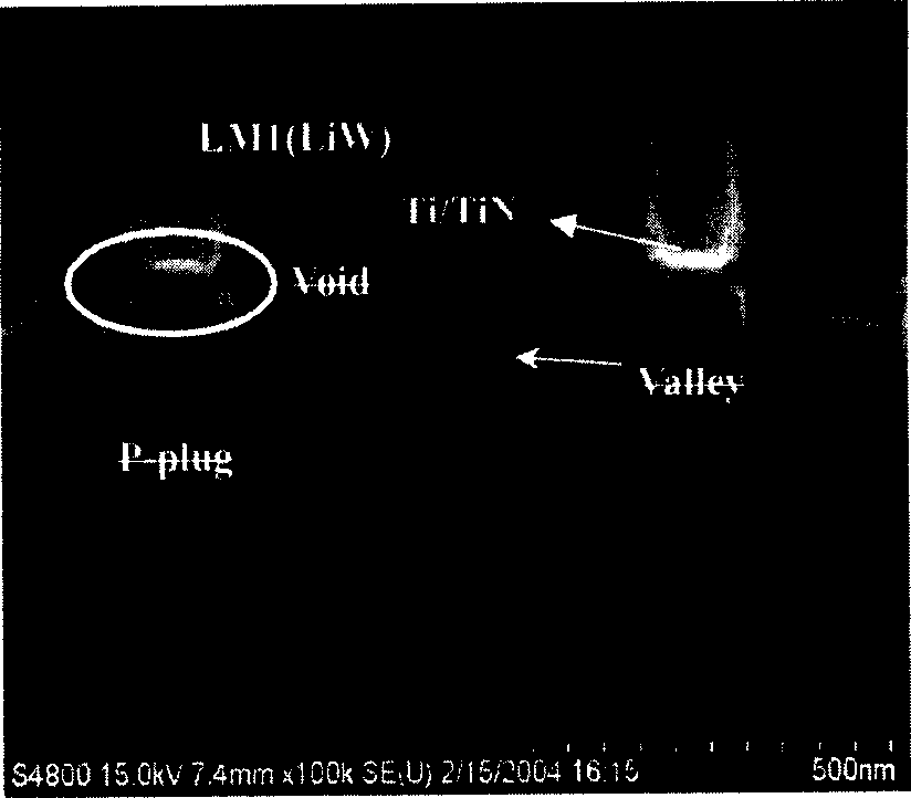
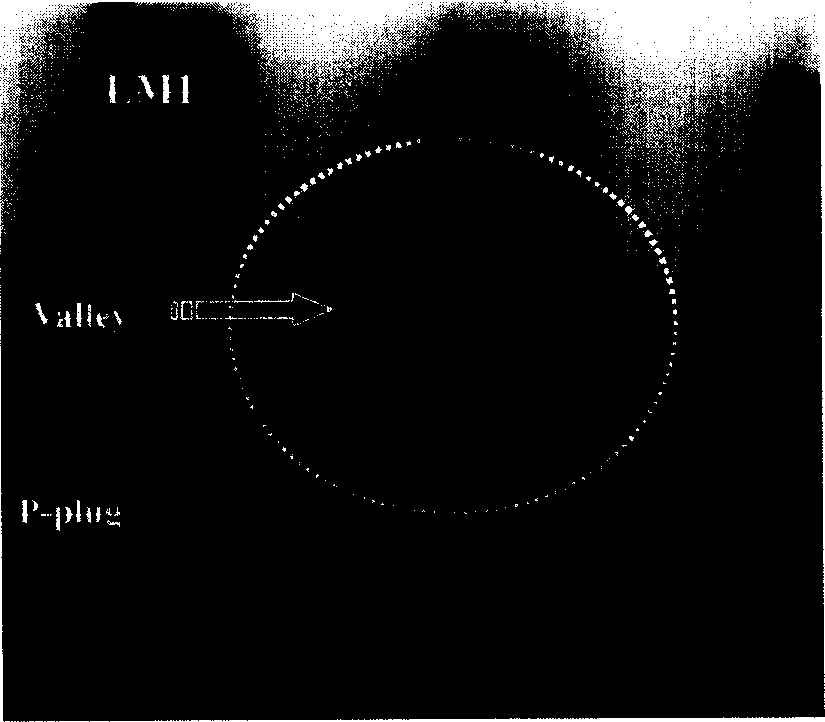
A semiconductor and device technology, applied in the field of preventing gaps between different materials in semiconductor devices, can solve the problems of incomplete corrosion of the W layer and inability to form memory unit contacts, etc., to eliminate the reduction in yield and stabilize the source and drain The effect of contact resistance

Inactive Publication Date: 2006-11-22
SEMICON MFG INT (SHANGHAI) CORP +1
View PDF0 Cites 4 Cited by
  • Summary
  • Abstract
  • Description
  • Claims
  • Application Information

AI Technical Summary

Problems solved by technology

[0021] In order to prevent gaps between the contact plugs and the memory cell contacts formed by the W layer, technicians attempt to reduce the corrosion effect of the plasma etching gas. As a result, the W layer cannot be completely etched and the required W layer composition cannot be formed. storage unit contacts

Method used


Image

  • Method for preventing clearance generation between different materials in semiconductor device
  • Method for preventing clearance generation between different materials in semiconductor device
  • Method for preventing clearance generation between different materials in semiconductor device

Examples


Embodiment Construction

[0066] see below Figure 10 to Figure 17 The method of the present invention is described in detail, taking the manufacturing method of the memory unit contacts in the 0.18 μm NAND flash memory as an example to describe the present invention in detail.

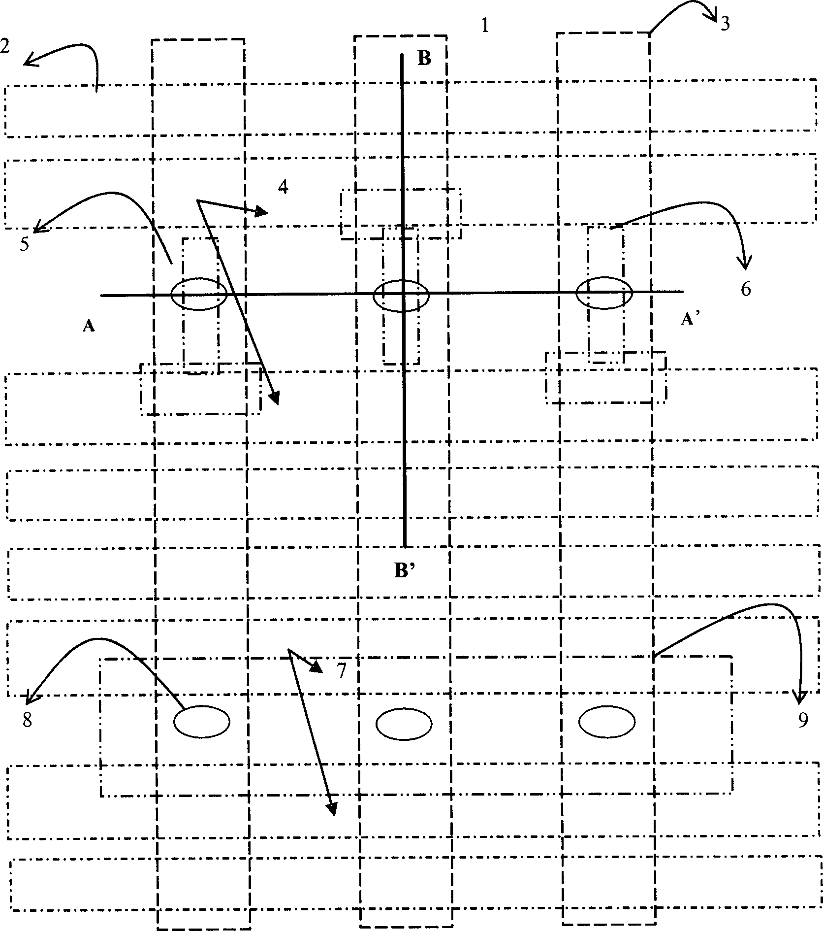
[0067] Figure 10 After determining the gate in the 0.18 μm “NAND” flash memory, the 0.18 μm “NAND” flash memory structure after depositing and reflowing phosphoborosilicate glass (BPSG) for the first time by the manufacturing method of the present invention figure 1 The schematic diagram of the cross-sectional structure cut by the B-B' line in the middle, and Figure 4 same;

[0068] Figure 11 It is the 0.18 μm "NAND" flash memory structure after the first photolithographic etching of the memory cell contact (CCT) according to the method of the present invention. figure 1 The cross-sectional schematic diagram cut by the line B-B′ in the middle, and Figure 5 same;

[0069] Figure 12 It is the 0.18 μm "NAND" flash mem...


PUM


Abstract

The invention discloses a gap avoiding method among semiconductors of different materials, which comprises the following steps: forming W layer with Ti-TiN-W stacked metal layer LM1 on the polysilicon touching piston; forming the second borophosphor silicate glass (BPSG) layer barrier layer on the polysilicon touching piston to prevent erosion LM1 layer with chlorine ion from eroding polysilicon touching piston. The invention can avoid gap between W layer storage unit contacts (CCT), when forming storage unit W layer contact.

Description

technical field [0001] The invention relates to a method for manufacturing a semiconductor device, in particular to a method for preventing gaps between different materials in the semiconductor device. Background technique [0002] A semiconductor device generally includes contact plugs for connecting various components and memory cell contacts disposed on the contact plugs. If the contact plug and the memory unit contact on it are made of different materials, since the materials for manufacturing the contact plug and the memory unit contact on it are different, when forming the pattern of the memory unit contact on it, The etchant used destroys the material of the contact plug, thereby creating a void between the contact plug and the memory cell contacts located thereon. The gap generated between the contact plug and the contact of the memory cell on it increases the contact resistance between the contact plug and the contact of the memory cell on it, which adversely affec...

Claims


Application Information

Patent Timeline
Patent Type & Authority Applications(China)
IPC IPC(8): H10B99/00H01L21/768
Inventor 申星勋蒋莉金钟雨
Owner SEMICON MFG INT (SHANGHAI) CORP
Learn More