Hard film layer dedicated for micro-bore of flexible printed circuit board
A technology of printed circuit and hard film layer, which is applied in the direction of drilling repair, layered products, drilling tool accessories, etc. It can solve the problems of low film density, poor bonding force between film and substrate, and low ionization rate of sputtering deposition. , achieve high thermal conductivity, increase bonding force, and high toughness
- Summary
- Abstract
- Description
- Claims
- Application Information
AI Technical Summary
Problems solved by technology
Method used
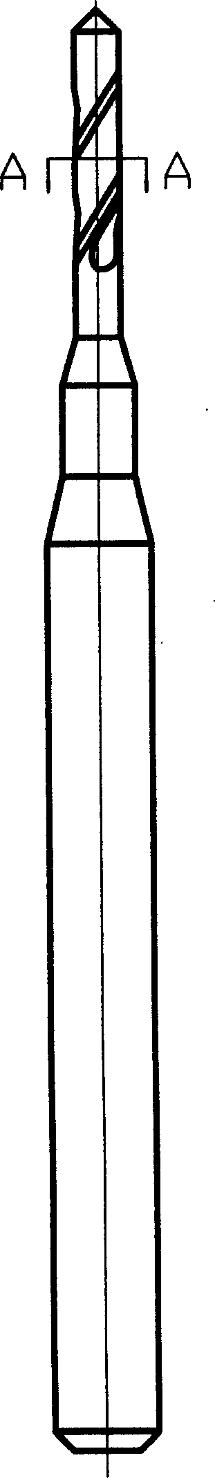
Image

Examples
Embodiment 1
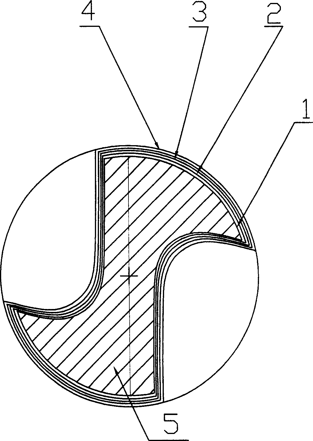
[0035] The film layer is CrN (chromium nitride). The number of layers of the film is three layers.
[0036] a. Transition layer Cr (chromium): the composition of this layer is all metal chromium, and the film thickness is 0.05 μm; b. Nitride transition layer: the ratio of Cr (chromium) metal to CrN (chromium nitride) is about 1: 8. The film thickness is about 0.1 μm; c. Nitride hard wear-resistant layer: the composition is CrN (chromium nitride), and the film thickness is about 0.6 μm.
Embodiment 2
[0038] The film layer is CrN (chromium nitride). The number of layers of the film is three layers.
[0039] a. Transition layer Cr (chromium): the composition of this layer is all metal chromium, and the film thickness is 0.1 μm; b. Nitride transition layer: the ratio of Cr (chromium) metal to CrN (chromium nitride) is about 1: 10. The film thickness is about 0.3 μm; c. Nitride hard wear-resistant layer: the composition is CrN (chromium nitride), and the film thickness is about 0.8 μm.
Embodiment 3
[0041] The film layer is CrTiAlN (chromium titanium aluminum nitrogen). The number of layers of the film is four.
[0042] The transition layer contains palladium, titanium and aluminum, wherein the ratio of chromium, titanium and aluminum is 60:1:0.6, and the film thickness is 0.05 μm;
[0043] The nitride transition layer includes an inner mixed layer 2 and an outer mixed layer 3 with a thickness of 0.1 μm and 0.4 μm respectively. The ratio of metal and metal nitride in the inner mixed layer 2 is controlled at 4:3, and the metal elements contained in it are chromium, titanium, The ratio of aluminum is 60:1:0.6; the ratio of metal and metal nitride in the outer mixed layer 3 is 0.5:3, and the ratio of the contained metal elements chromium, titanium and aluminum is controlled at 3:1:0.5.
[0044] Nitride hard wear-resistant layer, the composition of which is chromium, titanium, aluminum and nitrogen, and the film thickness is 0.5 μm. The nitride hard wear-resistant layer als...
PUM
| Property | Measurement | Unit |
|---|---|---|
| Film thickness | aaaaa | aaaaa |
| Film thickness | aaaaa | aaaaa |
| Film thickness | aaaaa | aaaaa |
Abstract
Description
Claims
Application Information
 - R&D
- Intellectual Property
- Life Sciences
- Materials
- Tech Scout
- Unparalleled Data Quality
- Higher Quality Content
- 60% Fewer Hallucinations
Browse by: Latest US Patents, China's latest patents, Technical Efficacy Thesaurus, Application Domain, Technology Topic, Popular Technical Reports.
© 2025 PatSnap. All rights reserved.Legal|Privacy policy|Modern Slavery Act Transparency Statement|Sitemap|About US| Contact US: help@patsnap.com