Plasma exciting method
A plasma and pulse excitation technology, applied in the fields of plasma, semiconductor/solid-state device manufacturing, electrical components, etc., can solve problems such as volume increase, uneven etching rate, asymmetry, etc., and achieve small difference in chemical reaction speed, The effect of reducing asymmetry and reducing damage
- Summary
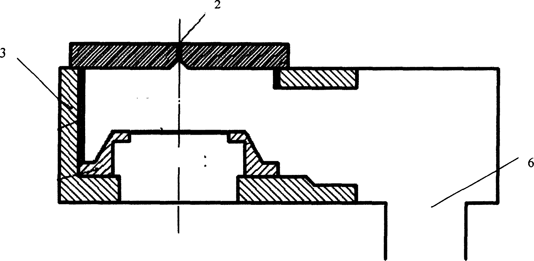
- Abstract
- Description
- Claims
- Application Information
AI Technical Summary
Problems solved by technology
Method used
Image

Examples
Embodiment 1
[0020] In the plasma excitation method of this embodiment, the upper electrode is excited in pulse mode, and the lower electrode is excited by radio frequency to apply a bias voltage to the substrate to control the ion energy reaching the substrate.
[0021] During specific implementation, coils in the prior art may be used. The upper electrode is connected with a pulse power supply, and the lower electrode is connected with a 13.56MHz radio frequency power supply. This excitation method reduces the inhomogeneity of the particle density distribution caused by the asymmetry of the gas flow distribution. This excitation method greatly reduces electron impact ionization during the afterglow. The diffusion of charged particles and excited species during the post-glow smooths out the asymmetry created by the previous pulse, providing more uniform initial conditions for the next pulse. Therefore, the use of pulse excitation can reduce the asymmetry of the azimuth angle and improve...
Embodiment 2
[0023] In the plasma excitation method of this embodiment, the upper electrode is excited by high-frequency radio frequency, and the lower electrode is excited by low-frequency radio frequency to apply a bias voltage to the substrate to control the ion energy reaching the substrate.
[0024] During specific implementation, coils in the prior art may be used. The upper electrode is connected to a high-frequency radio frequency power supply, wherein the frequency range is 10-200MHz, specifically in the present embodiment, the frequency point used is 27MHz; the lower electrode is connected to a low-frequency radio frequency power supply, wherein the frequency range is 1-5MHz, specifically in In this embodiment, the frequency point used is 2MHz.
[0025] Using such an excitation method can reduce the asymmetry of the azimuth angle and improve the uniformity of the plasma, so that the difference in the chemical reaction speed on the wafer surface is small, the etching rate is unifo...
Embodiment 3
[0027] In the plasma excitation method of this embodiment, the upper electrode is excited by high-frequency radio frequency, and the lower electrode is excited by pulses to apply a bias voltage to the substrate to control the ion energy reaching the substrate.
[0028] During specific implementation, the flat electrode in the prior art can be used. The upper electrode is connected with a high-frequency radio frequency power supply, and the frequency used is 100MHz; the lower electrode is connected with a pulse power supply.
[0029] Using such an excitation method can reduce the asymmetry of the azimuth angle and improve the uniformity of the plasma, so that the difference in the chemical reaction speed on the wafer surface is small, the etching rate is uniform, and the quality of the etched wafer is improved.
PUM
 Abstract
Description
Claims
Application Information
 - Generate Ideas
- Intellectual Property
- Life Sciences
- Materials
- Tech Scout
- Unparalleled Data Quality
- Higher Quality Content
- 60% Fewer Hallucinations
Browse by: Latest US Patents, China's latest patents, Technical Efficacy Thesaurus, Application Domain, Technology Topic, Popular Technical Reports.
© 2025 PatSnap. All rights reserved.Legal|Privacy policy|Modern Slavery Act Transparency Statement|Sitemap|About US| Contact US: help@patsnap.com