LED with high light extracting efficiency and preparing method thereof
A light-emitting diode, high-light extraction technology, applied in electrical components, circuits, semiconductor devices, etc., can solve the problems of photon loss, the light in the sidewall cannot be used, etc., achieve small absorption loss, improve light extraction efficiency, avoid voids and pinhole effect
- Summary
- Abstract
- Description
- Claims
- Application Information
AI Technical Summary
Problems solved by technology
Method used
Image
Examples
Embodiment Construction
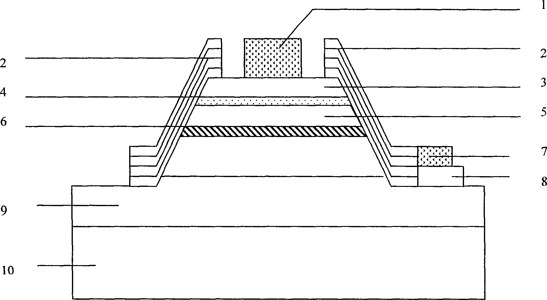
[0018] On a grown LED structure wafer, use sputtering or evaporation to grow the P-electrode ohmic contact layer 4 on the wafer P-type semiconductor 9. The P-electrode ohmic contact layer is made of Ni / Au, with a thickness of 40 Å and 70 Å respectively. . Use photoresist as a mask to carve out the LED table structure pattern on the wafer by photolithography, and then use the ion etching system ICP to carve out the LED table; after carving out the LED table, strip and remove the remaining photoresist; then Put the sample in a rapid annealing furnace, the P electrode ohmic contact layer 4 alloy, the condition is that the ratio of oxygen and nitrogen components is 4 at 500°C:
[0019] Rapid annealing in a gas mixture of 1 for 1 minute;
[0020] 1) Protect the P electrode ohmic contact layer 4 and the side of the LED table with glue by ordinary photolithography, and sputter a Ti / Al metal film on the N-type semiconductor 9 at the bottom of the LED table as the N electrode by sput...
PUM
 Abstract
Description
Claims
Application Information
 - R&D
- Intellectual Property
- Life Sciences
- Materials
- Tech Scout
- Unparalleled Data Quality
- Higher Quality Content
- 60% Fewer Hallucinations
Browse by: Latest US Patents, China's latest patents, Technical Efficacy Thesaurus, Application Domain, Technology Topic, Popular Technical Reports.
© 2025 PatSnap. All rights reserved.Legal|Privacy policy|Modern Slavery Act Transparency Statement|Sitemap|About US| Contact US: help@patsnap.com

