Method for reducing electric leakage of transistor in active zone edge junction
A technology of active regions and transistors, applied in the manufacture of circuits, electrical components, semiconductors/solid-state devices, etc., can solve problems such as large junction leakage, shallow junctions, blocking, etc., and achieve the effect of preventing junction leakage and deepening junction depth
- Summary
- Abstract
- Description
- Claims
- Application Information
AI Technical Summary
Problems solved by technology
Method used
Image
Examples
Embodiment Construction
[0019] The specific implementation manners of the present invention will be further described in detail below in conjunction with the accompanying drawings.
[0020] N+ ion implantation:
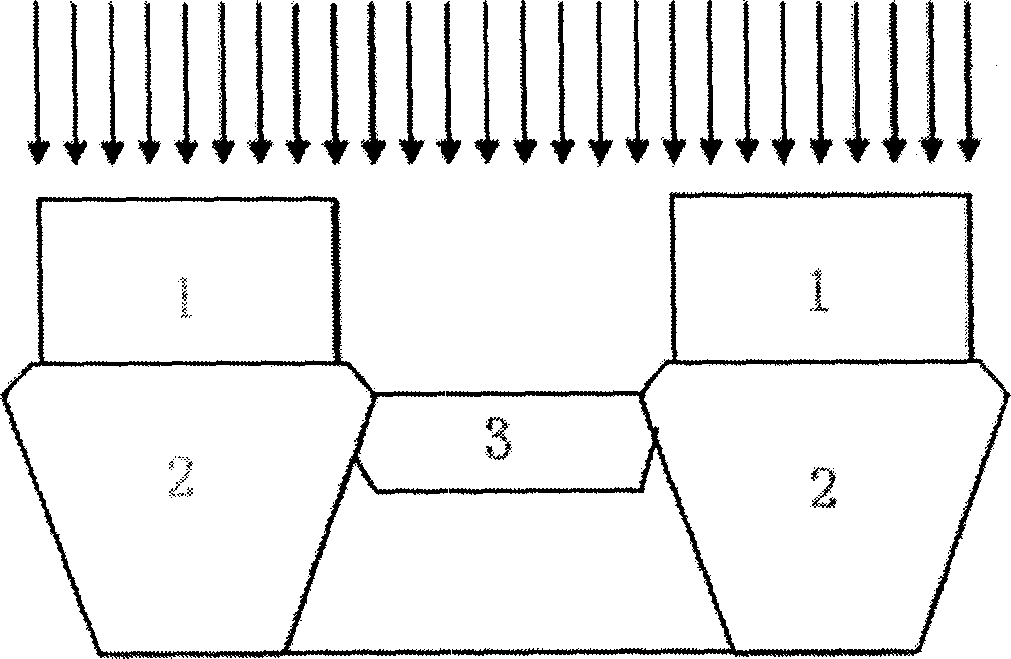
[0021] Firstly, by photolithography, the photoresist of all the N+ type active regions to be implanted on the semiconductor substrate is removed to expose the active regions.
[0022] Secondly, if figure 1 As shown, an N+ ion implantation is performed on the exposed active region, and the implantation angle is 0°.
[0023] Secondly, the remaining photoresist after photolithography is removed.
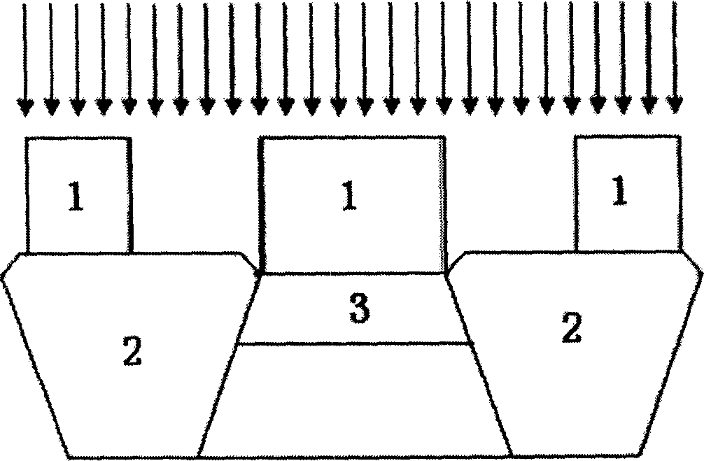
[0024] Next, through photolithography, remove the photoresist in the edge region of the active region within the range from the junction of the active region and the field region to the field region extending to the direction of the field region for 1 / 2 the length of the field region, exposing the edge region of the active region .
[0025] again, as figure 2 As shown, another N+ ion implantatio...
PUM
 Abstract
Description
Claims
Application Information
 - R&D
- Intellectual Property
- Life Sciences
- Materials
- Tech Scout
- Unparalleled Data Quality
- Higher Quality Content
- 60% Fewer Hallucinations
Browse by: Latest US Patents, China's latest patents, Technical Efficacy Thesaurus, Application Domain, Technology Topic, Popular Technical Reports.
© 2025 PatSnap. All rights reserved.Legal|Privacy policy|Modern Slavery Act Transparency Statement|Sitemap|About US| Contact US: help@patsnap.com


