Manufacture method of contact hole and manufacture method of semiconductor element

A manufacturing method and contact hole technology, applied in semiconductor/solid-state device manufacturing, electrical components, circuits, etc., can solve problems such as complex process, substrate surface damage, junction leakage, etc., to increase the process window, ensure uniformity, The effect of simplifying the process steps

Inactive Publication Date: 2007-01-24
PROMOS TECH INC
View PDF4 Cites 0 Cited by
  • Summary
  • Abstract
  • Description
  • Claims
  • Application Information

AI Technical Summary

Problems solved by technology

[0013] Therefore the purpose of the present invention is to provide a method for manufacturing a contact hole, to solve the problem that the surface of the substrate is easily damaged in the process of the known bit line contact hole, resulting in junction leakage.
[0014] Another object of the present invention is to provide a method for manufacturing a contact hole, to solve the disadvantages that the process of the known bit line contact hole is complicated

Method used


Image

  • Manufacture method of contact hole and manufacture method of semiconductor element
  • Manufacture method of contact hole and manufacture method of semiconductor element
  • Manufacture method of contact hole and manufacture method of semiconductor element

Examples


Embodiment Construction

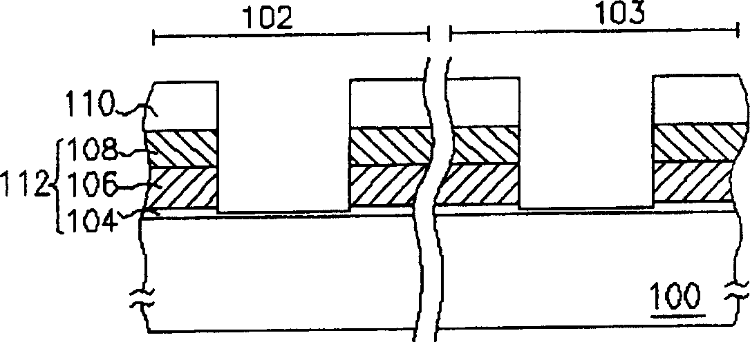
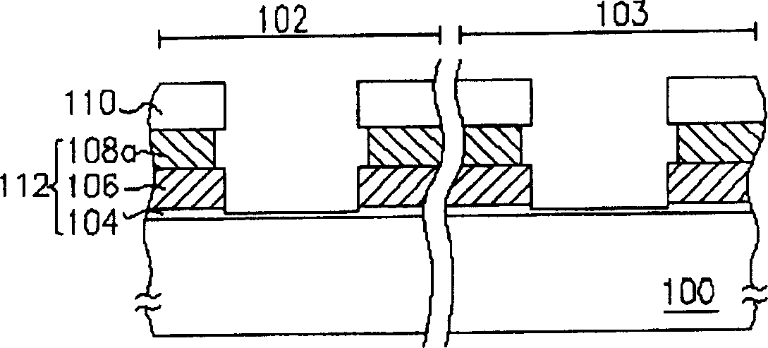
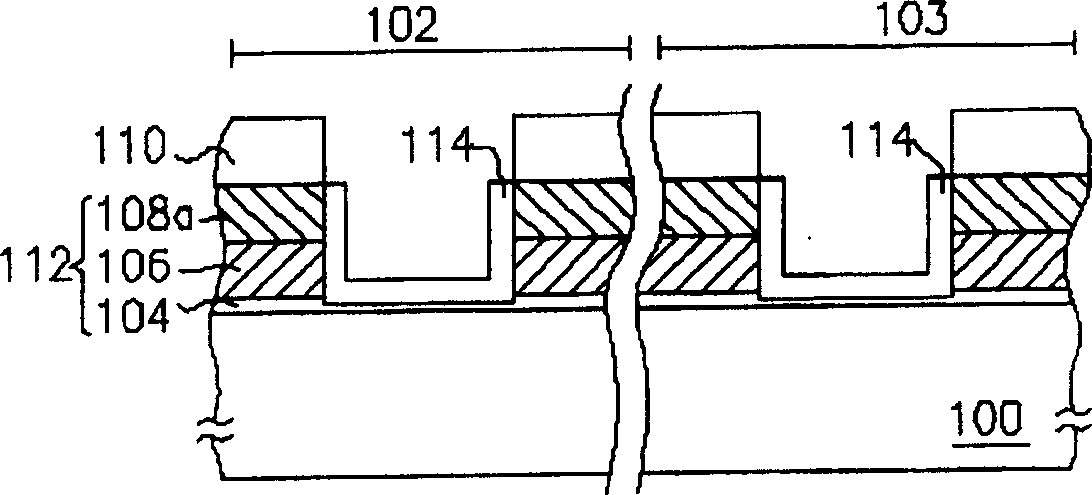
[0042] Figure 2A to Figure 2F Shown is a cross-sectional view of a manufacturing process of a contact hole according to a preferred embodiment of the present invention.

[0043] Please refer to Figure 2A Firstly, a substrate 100 is provided, on which several conductive structures 112 have been formed, and a top cover layer 110 is formed on the top of the conductive structures 112 . Wherein, the area 102 marked in the figure is the area where the bit line contact hole is planned to be formed later, and the area 103 is the area where the bit line contact hole is not planned to be formed later. Therefore, the area 102 is the area where the bit line contact hole is planned to be formed in the memory cell area, and the area 103 is, for example, the area where the bit line contact hole is not expected to be formed in the peripheral circuit area or the memory cell area.

[0044]In a preferred embodiment, the conductive structure 112 is, for example, a gate structure, which is com...


PUM


Abstract

The method includes following structure: first, forming several conduction structures on substrate provided; next, carrying out step of ion implantation; then, carrying out heat process in order to form lining on sidewall of conduction structure and on surface of substructure uncovered by conduction structure, and thickness of lining formed on sidewall is less than thickness of lining formed on surface of substructure; forming gap wall on two sides of the said conduction structure; finally, forming insulating layer above the substrate, and patternizing the insulating layer in order to form contact hole between two conduction structures. Since thickness of lining formed on sidewall of conduction structure is thinner, thus subsequent etching for lining on sidewall is not needed so as to ensure evenness of thickness of lining of surface of substrate.

Description

technical field [0001] The invention relates to a method for manufacturing a semiconductor, in particular to a method for manufacturing a contact hole and a method for manufacturing a semiconductor element. Background technique [0002] With the advancement of semiconductor technology, the size of components is also continuously reduced, entering the field of deep submicron. When the integration level of the integrated circuit increases, the surface of the wafer cannot provide enough area to make the required interconnection (Interconnect). The design of the metal interconnection line becomes a necessary method for very large scale integrated circuit (VLSI) technology. In addition, if different metal layers are to be connected, an opening must be dug in the insulating layer between the two metal layers and filled with conductive material to form a plug structure that connects the two metal layers. [0003] In order to overcome the ever-smaller line width and prevent misali...

Claims


Application Information

Patent Timeline
Patent Type & Authority Patents(China)
IPC IPC(8): H01L21/768H01L21/30H01L21/265
Inventor 叶芳裕陈俊哲
Owner PROMOS TECH INC
Why Eureka
Try Eureka