Method of manufacturing dielectric layer of grid

A technology for a gate dielectric layer and a manufacturing method, which is applied in the field of semiconductor component manufacturing, can solve the problems of reducing component stability and reliability, reducing process yield, increasing power consumption, etc., so as to avoid thinning and improve reliability. and stability, the effect of preventing junction leakage

Inactive Publication Date: 2008-04-02
POWERCHIP SEMICON CORP
View PDF2 Cites 0 Cited by
  • Summary
  • Abstract
  • Description
  • Claims
  • Application Information

AI Technical Summary

Problems solved by technology

The neck junction effect will reduce the quality of the components, reduce the stability and reliability of the components, and lead to a decrease in the yield of the process
However, in the low-voltage circuit area 102, due to the presence of the recess 168, doped polysilicon will fill the region of the recess 168, and problems such as junction leakage will occur, which not only increases power consumption, but also lengthens the life of the device. calculating speed

Method used


Image

  • Method of manufacturing dielectric layer of grid
  • Method of manufacturing dielectric layer of grid
  • Method of manufacturing dielectric layer of grid

Examples


Embodiment Construction

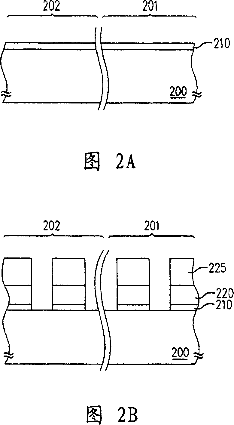
[0046] 2A to 2F are cross-sectional views illustrating a manufacturing process of a gate dielectric layer according to a preferred embodiment of the present invention.

[0047] Please refer to FIG. 2A , in this manufacturing method, for example, a substrate 200 is firstly provided, and the substrate 200 can be at least divided into a high-voltage circuit area 201 and a low-voltage circuit area 202 . Then, for example, RCA solution (ammonia NH 4 OH and hydrogen peroxide H 2 o 2mixed solution) to perform a cleaning step on the substrate 200. Afterwards, a dielectric layer 210 is formed on the substrate 200 . The dielectric layer 210 is used as a gate dielectric layer in the high-voltage circuit region 201 , so the thickness of the dielectric layer 210 is thicker than the existing pad oxide layer, and the thickness of the dielectric layer 210 is about 200˜1000 angstroms. The forming method of the dielectric layer 210 is, for example, a thermal oxidation method.

[0048] Afte...


PUM


Abstract

The method includes steps: first, the provided substrate can at least be divided into region of high voltage circuit and region of low voltage circuit; next, forming first dielectric layer on substrate, and the first dielectric layer is in use for grid dielectric layer in region of high voltage circuit; then, forming mask layer on the first dielectric layer, patterning the mask layer, the first dielectric layer, and the substrate in order to form groove in the substrate; forming insulating layer on the substrate to fill in the groove; removing the mask layer, and partial insulating layer to expose surface of the first dielectric layer; removing the first dielectric layer in region of low voltage circuit to expose surface of the substrate; forming second dielectric layer in substrate of the region of low voltage circuit' the thickness of the second dielectric layer is smaller than the first dielectric layer.

Description

technical field [0001] The invention relates to a method for manufacturing a semiconductor element, in particular to a method for manufacturing a gate dielectric layer. Background technique [0002] With the rapid development of the field of integrated circuits, high performance, high integration, low cost, light weight and short size have become the goals pursued by the design and manufacture of electronic products. For the current semiconductor industry, in order to meet the above goals, it is often necessary to manufacture components with multiple functions on the same chip. [0003] Integrating high-voltage components and low-voltage components on the same chip is a way to achieve the above requirements. For example, low-voltage components are used to manufacture control circuits, and high-voltage components are used to manufacture programmable read-only memory (EPROM), flash memory (Flash Memory) or driving circuits of liquid crystal displays. [0004] However, in ord...

Claims


Application Information

Patent Timeline
Patent Type & Authority Patents(China)
IPC IPC(8): H01L21/82
Inventor 陈文吉陈东波薛凯安郑胜鸿
Owner POWERCHIP SEMICON CORP
Why Eureka
Try Eureka