Method for reducing electric leakage of transistor in active zone edge junction

An active area and transistor technology, applied in the manufacturing of circuits, electrical components, semiconductor/solid-state devices, etc., can solve the problems of large junction leakage, blocking, and easy junction leakage, and achieve the effect of deepening the junction depth and preventing junction leakage.

Inactive Publication Date: 2009-04-08
SHANGHAI INTEGRATED CIRCUIT RES & DEV CENT +1
View PDF5 Cites 0 Cited by
  • Summary
  • Abstract
  • Description
  • Claims
  • Application Information

AI Technical Summary

Problems solved by technology

Since the cross-section of the shallow trench region is an inverted trapezoid, the field oxygen at the edge of the shallow trench will block the impurity implantation, resulting in a shallower PN junction at the edge of the active region, resulting in a larger junction leakage.
figure 1 It is a junction formed after conventional source-drain implantation. It can be seen that near the edges of both sides of the active region, because the field oxygen at the edge of the shallow groove blocks the impurity implantation, the formed junction is relatively shallow, and junction leakage is more likely to occur.

Method used


Image

  • Method for reducing electric leakage of transistor in active zone edge junction
  • Method for reducing electric leakage of transistor in active zone edge junction

Examples


Embodiment Construction

[0019] The specific implementation manners of the present invention will be further described in detail below in conjunction with the accompanying drawings.

[0020] N+ ion implantation:

[0021] Firstly, by photolithography, the photoresist of all the N+ type active regions to be implanted on the semiconductor substrate is removed to expose the active regions.

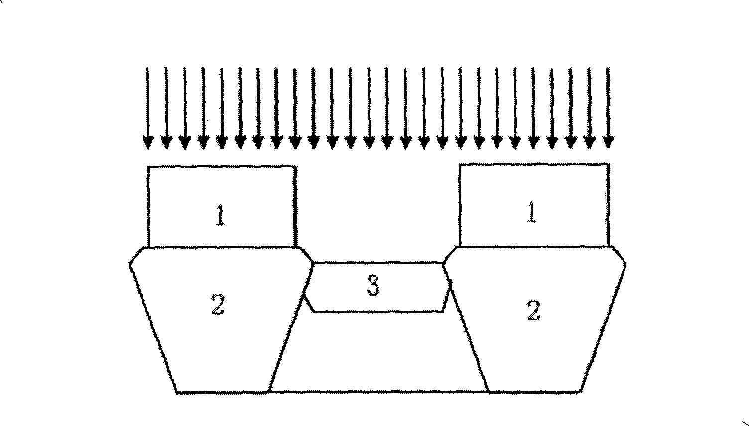
[0022] Secondly, if figure 1 As shown, an N+ ion implantation is performed on the exposed active region, and the implantation angle is 0°.

[0023] Secondly, the remaining photoresist after photolithography is removed.

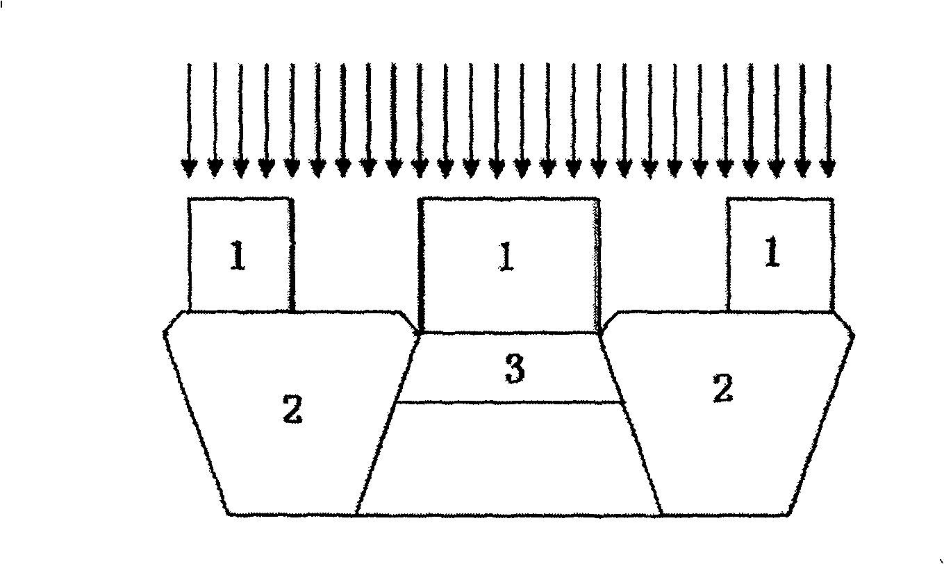
[0024] Next, through photolithography, remove the photoresist in the edge region of the active region within the range from the junction of the active region and the field region to the field region extending to the direction of the field region for 1 / 2 the length of the field region, exposing the edge region of the active region .

[0025] again, as figure 2 As shown, another N+ ion implantatio...


PUM


Abstract

The invention discloses a method for reducing junction leakage on the edge of the active region of a transistor, comprising the steps of: developing to eliminate photoetching glue on the edge of the active region by photoetching after routine source / drain injection, and making a supplemental ion injection on the exposed edge of the active region to deepen the junction on the edge of the active region so as to effectively prevent the junction leakage.

Description

technical field [0001] The invention relates to a shallow trench isolation process method, in particular to a method for reducing transistor leakage at the edge junction of an active region during source and drain injection in the shallow trench isolation process. Background technique [0002] The static power consumption of the circuit is mainly composed of the subthreshold current of the transistor and the junction leakage. With the continuous development of integrated circuits, the integration of circuits is getting higher and higher, and more and more transistors are integrated in a single circuit. To reduce the static power consumption of the circuit, the subthreshold current and junction leakage of a single transistor must be reduced. [0003] For the integrated circuit manufacturing process using shallow trench isolation, during source and drain implantation, the photoresist layer on the surface of the active region to be implanted is removed through a photolithograph...

Claims


Application Information

Patent Timeline
Patent Type & Authority Patents(China)
IPC IPC(8): H01L21/76H01L21/265H01L21/8234
Inventor 顾学强
Owner SHANGHAI INTEGRATED CIRCUIT RES & DEV CENT
Why Eureka
Try Eureka