Contact hole manufacturing method

A manufacturing method and technology of contact holes, which are used in semiconductor/solid-state device manufacturing, electrical components, circuits, etc., can solve problems such as piercing, junction leakage, and increase in contact resistance, so as to eliminate inconsistencies in loss, prevent junction leakage, and improve contact. effect of effect

Active Publication Date: 2021-08-10
SHANGHAI HUALI INTEGRATED CIRCUTE MFG CO LTD
View PDF22 Cites 0 Cited by
  • Summary
  • Abstract
  • Description
  • Claims
  • Application Information

AI Technical Summary

Problems solved by technology

Simultaneously, described second etch also needs to carry out over-etch and guarantee that the natural oxide layer 5 on the surface of described metal silicide 4 is completely removed, but, because the size of different pattern regions such as source region, drain region or polysilicon gate 3 When the size is different, the thickness of the natural oxide layer 5 will be different, and the second etching needs to ensure that the thickest natural oxide layer 5 is removed, so the metal silicide 4 in the thinner area of ​​the natural oxide layer 5 will inevitably be overgrown. etch, as the technology node shrinks, the metal silicide 4 will even be etched through
When the metal silicide 4 is over-etched to produce thickness loss, the contact resistance between the metal of the contact hole 8 and the metal silicide 4 will increase; when the metal silicide 4 is etched through , prone to junction leakage

Method used


Image

  • Contact hole manufacturing method
  • Contact hole manufacturing method
  • Contact hole manufacturing method

Examples


Embodiment Construction

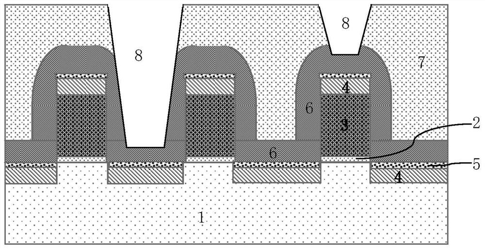
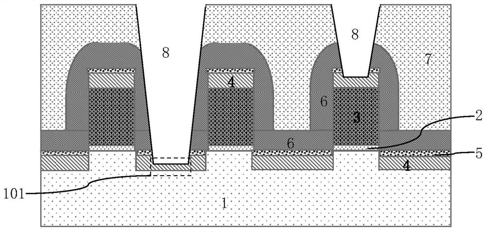
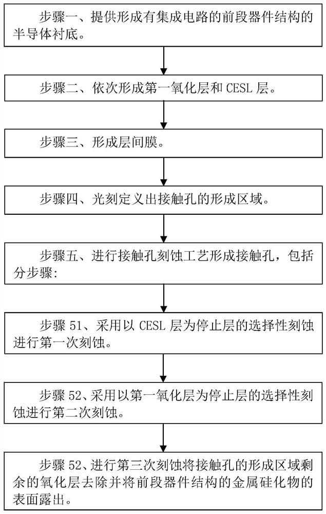
[0052] like figure 2 Shown is the flow chart of the manufacturing method of the contact hole in the embodiment of the present invention; as Figure 3A to Figure 3C Shown is a device structure diagram in each step of the manufacturing method of the contact hole in the embodiment of the present invention. The manufacturing method of the contact hole in the embodiment of the present invention includes the following steps:

[0053] Step 1, such as Figure 3A As shown, a semiconductor substrate 1 is provided, and a front-end device structure of an integrated circuit is formed on the semiconductor substrate 1. The front-end device structure includes a metal silicide 4 formed on the surface of the doped region that needs to be extracted, so The metal silicide 4 is used for metal contact with the subsequently formed contact hole 8, and a natural oxide layer 5 is formed on the surface of the metal silicide 4, and the natural oxide layer 5 is formed according to the pattern of the met...


PUM


Abstract

The invention discloses a method for manufacturing a contact hole, comprising steps: step 1, providing a semiconductor substrate with a front-end device structure of an integrated circuit; step 2, forming a first oxide layer and a CESL layer in sequence; step 3, forming a layer Interlayer film; Step 4, photolithography defines the formation area of ​​the contact hole; Step 5, performs a contact hole etching process to form a contact hole, including sub-steps: Step 51, using the CESL layer as a stop layer for selective etching to perform the second step Etching once; step 52, using the first oxide layer as a stop layer for selective etching to perform second etching; step 52, performing third etching to remove the remaining oxide layer in the formation area of ​​the contact hole and Expose the surface of the metal silicide in the front-stage device structure. The invention can reduce the loss of metal silicide at the bottom of the contact hole corresponding to each pattern and improve the consistency of loss, thereby reducing contact resistance and preventing junction leakage caused by metal silicide scratching.

Description

technical field [0001] The invention relates to a method for manufacturing a semiconductor integrated circuit, in particular to a method for manufacturing a contact hole. Background technique [0002] At each technology node of semiconductor integrated circuits, contact hole (CT) technology is a challenging and difficult point. It is a key step in connecting front-end devices and back-end metal wiring. He not only needs a low resistance value similar to the back-end wiring, but also ensures a good connection with the front-end device: it cannot be etched enough to cause an open circuit, and at the same time, it is necessary to control the loss (loss) of metal silicides such as NiSi to prevent metal silicide. The material is etched through (ETCH through) and thus causes the resistance value to increase and even the junction (Junction) leakage; in the process below the 45nm technology node, NiSi is usually used as the metal silicide. In order to solve this problem, the existi...

Claims


Application Information

Patent Timeline
Patent Type & Authority Patents(China)
IPC IPC(8): H01L21/768H01L21/8234
CPCH01L21/76802H01L21/76805H01L21/823475
Inventor 严磊孙淑苗
Owner SHANGHAI HUALI INTEGRATED CIRCUTE MFG CO LTD
Why Eureka
Try Eureka