
Method for avoiding ZEP520 electronic resist to generate cracks

A ZEP520, resist technology, applied in the field of microelectronics, can solve the problems of ZEP520 cracks, HMDS toxicity, environmental pollution, etc., to achieve the effect of improving yield, avoiding environmental pollution, and reducing costs

Inactive Publication Date: 2006-08-09
INST OF MICROELECTRONICS CHINESE ACAD OF SCI
View PDF0 Cites 3 Cited by
  • Summary
  • Abstract
  • Description
  • Claims
  • Application Information

AI Technical Summary

Problems solved by technology

Usually, a tackifier such as hexamethyldisilazane (HMDS) is vapor-deposited on the surface of the wafer, and there are two problems in this method: one is that HMDS itself is poisonous, and it is easy to cause human injury and environmental pollution. , Second, in order to make HMDS have a good effect of enhancing adhesion, a special fumigation furnace is required
As for how to avoid cracks in ZEP520, there is no corresponding solution at present

Method used


Image

  • Method for avoiding ZEP520 electronic resist to generate cracks
  • Method for avoiding ZEP520 electronic resist to generate cracks

Examples


Embodiment Construction

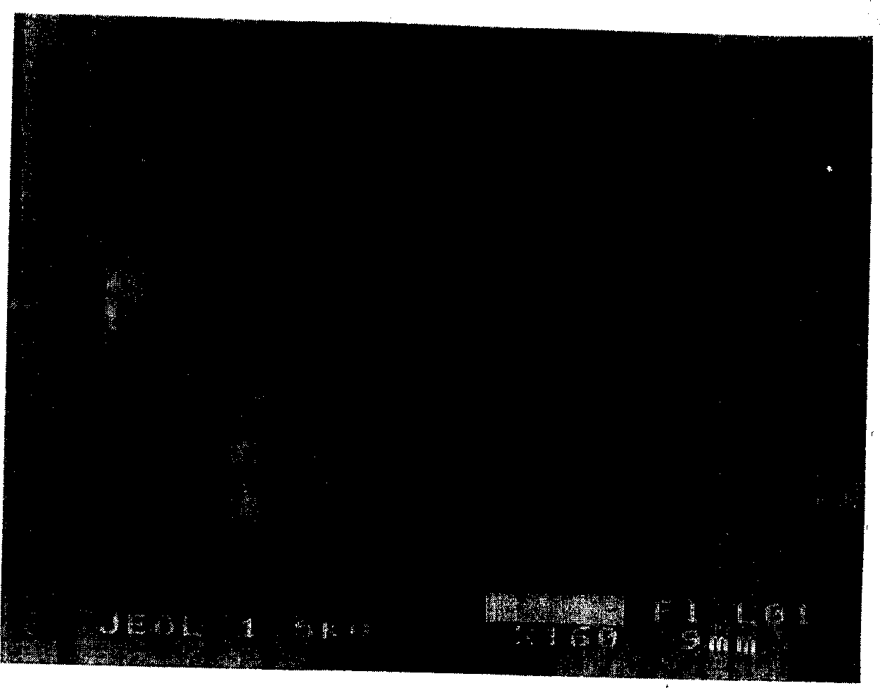
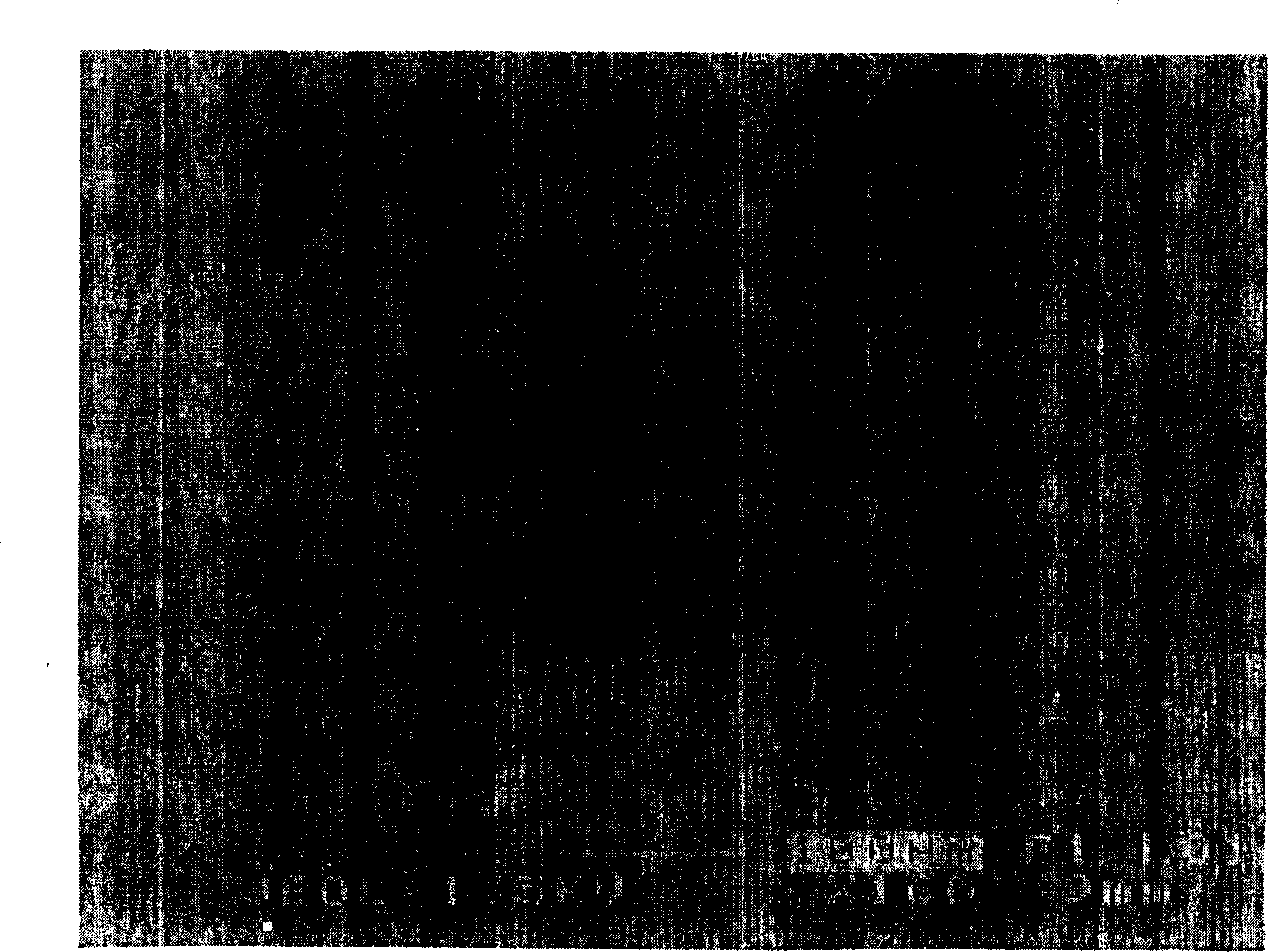
[0021] Concrete method of the present invention is not fumigation HMDS before coating ZEP520 electronic resist, but adopts physical method to carry out thermal treatment to the surface of substrate, then coats ZEP520 electronic resist immediately and can avoid the phenomenon that produces crack ( figure 2 ).

[0022] The substrate is mainly for gallium arsenide (GaAs) substrates. When using silicon (Si), indium phosphide (InP) and other substrates, in order to prevent cracks, it is best to heat-treat before coating ZEP520 electronic resist.

[0023] The time interval between heat treatment and gluing should be as short as possible, preferably within 5 seconds.

[0024] The specific method and principle of the present invention will be further described in detail by describing specific embodiments below in conjunction with the accompanying drawings, wherein:

[0025] figure 1 It is a scanning electron microscope (SEM) surface topography photograph of widely distributed crack...


PUM


Abstract

Fine graphics in Nano level can be prepared by using ZEP520 positivity electronic resist and electron beam write through photo etching. But, cracks are generated easily in resist in traditional technique, especially on substrate of gallium arsenide. There is no relevant solution for the problem. The disclosed method carries out heat treatment for substrate of wafer first; and then the method coats ZEP520 glue instantly so as to prevent ZEP520 from generation of cracks, as well as prevent poisonous tackifier HMDS from use. Advantages are: simple operation, convenience and reliable.

Description

technical field [0001] The present invention relates to the technical field of microelectronics, in particular, relates to a kind of commonly used positive electronic resist ZEP520 (chemical composition is α-chloromethacrylate ( α-chloromethacrylate) and α-methylstyrene (α-methyl styrene copolymer), which directly affects the processing effect of the final nanoscale graphic structure. Background technique [0002] In the field of microelectronics technology, the use of electron beam direct writing lithography to process nanoscale high-resolution graphic structures is an important means of nanoprocessing. The principle is: the polymer materials in the electronic resist are subjected to high-energy electron beams. The bombardment produces reactions such as chain scission (positive resist) or crosslinking (negative resist), and the solubility in the developer changes, which makes the dissolution rate of the exposed area and the unexposed area different, with a large The region...

Claims


Application Information

Patent Timeline
IPC IPC(8): G03F7/20H01L21/00
Inventor 龙世兵李志刚谢常青刘明陈宝钦
Owner INST OF MICROELECTRONICS CHINESE ACAD OF SCI
Learn More