Process for manufacturing 0.8 micron silicon bipolar CMOS integrated circuit

A manufacturing process and process technology, applied in the field of 0.8 micron silicon bipolar complementary metal oxide semiconductor integrated circuit manufacturing process, can solve the problems of high cost and complex process flow, and achieve the effect of high resistance and high gain

Active Publication Date: 2006-02-15
ADVANCED SEMICON MFG CO LTD
View PDF0 Cites 6 Cited by
  • Summary
  • Abstract
  • Description
  • Claims
  • Application Information

AI Technical Summary

Problems solved by technology

[0005] Aiming at the defects of complex process flow and high cost in the prior art, the purpose of the present invention is to provide an improved manufacturing process of 0.8 micron BICMOS integrated circuit, simplify the process flow, and reduce the cost of the process

Method used


Image

  • Process for manufacturing 0.8 micron silicon bipolar CMOS integrated circuit
  • Process for manufacturing 0.8 micron silicon bipolar CMOS integrated circuit
  • Process for manufacturing 0.8 micron silicon bipolar CMOS integrated circuit

Examples


Embodiment Construction

[0024] The technical solution of the present invention will be further described below in conjunction with the embodiments.

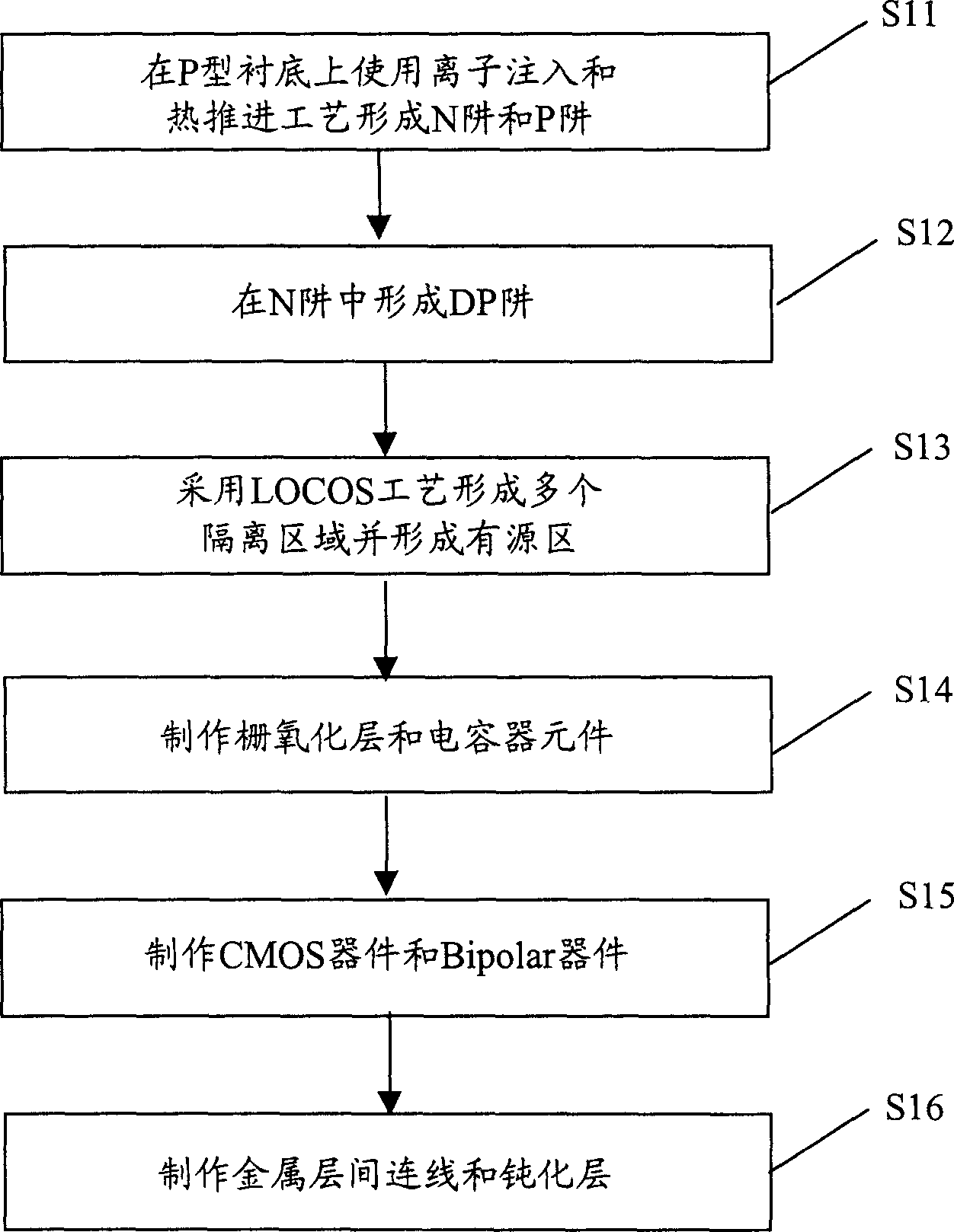
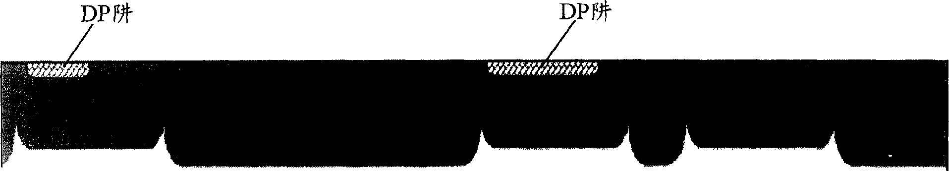
[0025] The flow process of manufacturing process of the present invention is as follows, with reference to figure 1 , the main features of which are that DP wells are also formed in N wells; the gate oxide layers of high-voltage devices and low-voltage devices are completed in the same oxidation step; and isolation NMOS devices and Bipolar NPN devices are formed on N wells with DP wells.

[0026] Such as figure 1 As shown, the process includes the following steps:

[0027] S11. Forming an N well and a P well on a P-type substrate by using ion implantation and a thermal push process. In this embodiment, the step of making the double wells specifically includes: initial oxygen; using photoresist to locate the N well region and the P well; N well ion implantation; P well ion implantation; double well advance. The above steps refer to figure 2 , these ...


PUM


Abstract

This invention discloses a improved 0.8um BICMOS IC manufacture technique to form DP trap in N trap, which comprises following steps: forming N trap and P trap on P-type substrate by ion implantation and thermal propulsion techniques; form DP trap in N trap: first, using photoresist to define the zone for DP trap, then forming DP trap by ion implantation; using LOCOS technique to form a plurality of separation zones with place same to formed trap and active region; preparing grid oxide layer and capacitor, wherein, the oxide layers for high-voltage and low-voltage devices are completed on same step; preparing CMOS device and Bipolar device; forming insulated NMOS and Bipolar NPN device on N trap with DP trap; manufacturing connecting wire between metal layers and passivation layer. The invention can simplify process and decrease cost.

Description

technical field [0001] The invention relates to a manufacturing process of a silicon bipolar complementary metal oxide semiconductor (BICMOS) integrated circuit, more specifically, a manufacturing process of a 0.8-micron BICMOS integrated circuit. Background technique [0002] At present, CMOS devices and Bipolar devices are mainly used in integrated circuits. These two devices have their own advantages and limitations. CMOS devices have the advantages of low power consumption, high integration and strong anti-interference ability, but they also have the advantages of device operating speed. The disadvantages of low and poor driving ability. Bipolar devices have the advantages of fast device speed, strong driving capability, and high simulation accuracy, but they also have the disadvantages of high device power consumption and low integration. From the above, it can be seen that the advantages and disadvantages of CMOS and Bipolar devices are just complementary. Therefore, ...

Claims


Application Information

Patent Timeline
Patent Type & Authority Applications(China)
IPC IPC(8): H01L21/8249
Inventor 乔琼华邵凯龚大卫
Owner ADVANCED SEMICON MFG CO LTD
Why Eureka
Try Eureka