Vertical-type power metal oxide semiconductor device with excess current protective function

An oxide semiconductor, vertical technology, used in semiconductor devices, semiconductor/solid-state device manufacturing, semiconductor/solid-state device components, etc., and can solve problems such as thermal damage

Inactive Publication Date: 2005-08-10
NEC ELECTRONICS CORP
View PDF1 Cites 0 Cited by
  • Summary
  • Abstract
  • Description
  • Claims
  • Application Information

AI Technical Summary

Problems solved by technology

Otherwise, when a short circuit occurs in the electric load circuit, overcurrent flows through the vertical type power MOS device so that it is thermally damaged

Method used


Image

  • Vertical-type power metal oxide semiconductor device with excess current protective function
  • Vertical-type power metal oxide semiconductor device with excess current protective function
  • Vertical-type power metal oxide semiconductor device with excess current protective function

Examples


no. 1 example

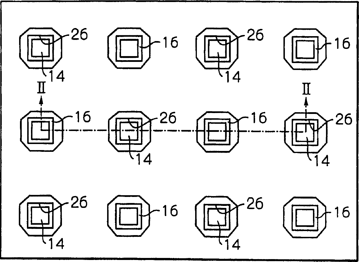
[0088] Referring to FIGS. 11A to 11J , a production method for producing the first embodiment of the vertical type power MOS device according to the present invention will now be explained.

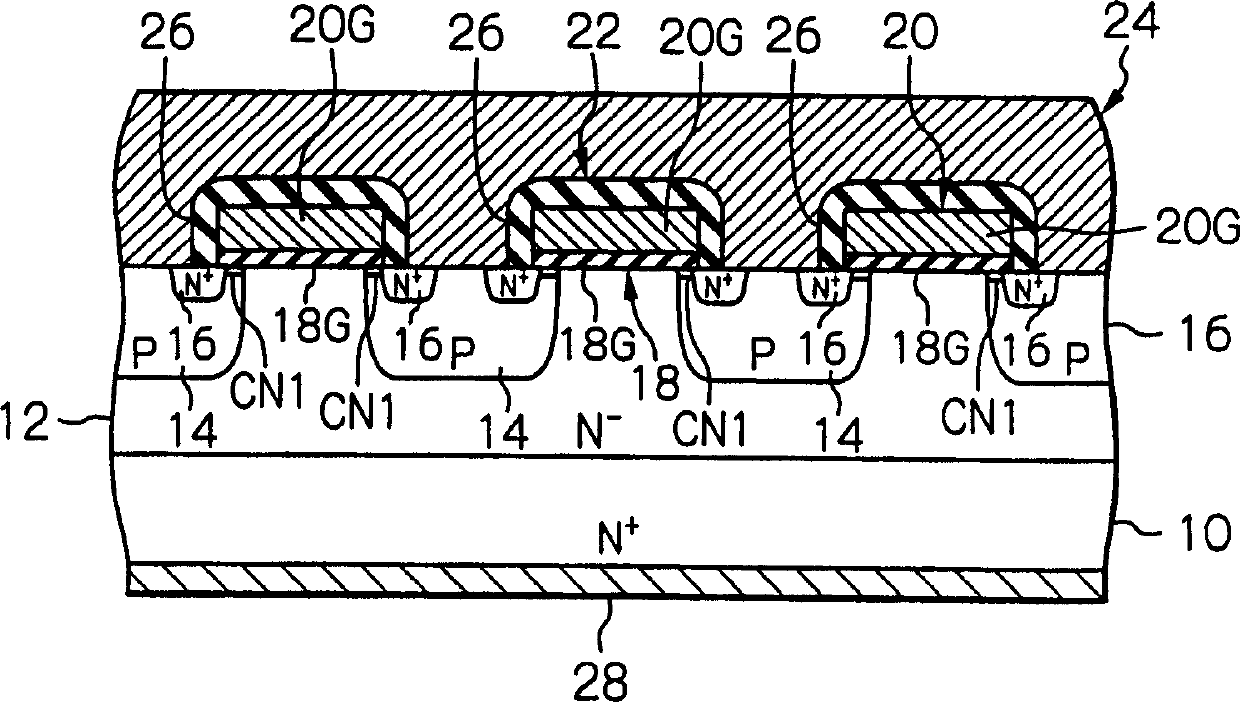
[0089] First, as shown in Figure 11A, N + type semiconductor substrate 112, and N - Type epitaxial layer 114 is formed as N + N on the type semiconductor substrate 112 - type drift layer. For example, from such as arsenic (As + ) and other N-type impurities such as N + type monocrystalline silicon wafer obtained N + type semiconductor substrate 122, and a plurality of chip areas in which vertical type power MOS devices will be fabricated are limited to N by scribing + type semiconductor substrate 122. Moreover, N - Type epitaxial layer or drift layer 114 contains N-type impurities, such as arsenic (As + )Wait.

[0090] After completing the N - After the formation of the type drift layer 114, as shown in FIG. 11B, by using photolithography process and wet or dry etching process ...

no. 2 example

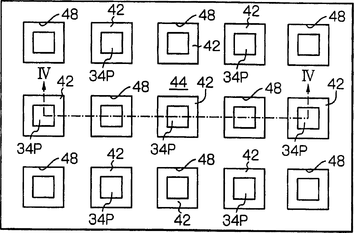
[0119] Referring to FIGS. 18A to 18D , the production method of the second embodiment for producing the vertical type power MOS device according to the present invention will be described below.

[0120] This production method includes first, second, third, fourth, fifth and sixth representative steps, which are substantially the same as those in the first production method mentioned as shown in FIGS. 11A to 11F . Note that in FIG. 18A , the same reference numerals as in FIG. 11F denote the same elements.

[0121] After completing the definition of the P-type low-density impurity implantation region 128L (FIG. 11F), a photoresist layer 146 is formed on the silicon dioxide layer 126, and the The photoresist layer 146 is patterned so that a portion of the P-type low-density impurity implantation region 128L is masked with the patterned photoresist layer 146, as shown in FIG. 18A. Note that in this figure, only two P-type low-density impurity implanted regions 128L are represent...


PUM


Abstract

The invention discloses a vertical type power metal-oxide-semiconductor device, which comprises a semiconductor substrate (112) and a plurality of transistor units (142H, 142L) arranged on the semiconductor substrate; wherein, the transistor units (142H, 142L) are electrically connected in parallel with each other; the transistor units are divided into at least two groups, the gate threshold voltage of the first group of the transistor units (142H) is higher than the second group of the transistor units (142L).

Description

technical field [0001] The invention relates to a vertical power metal oxide semiconductor (MOS) device with overcurrent protection function. Background technique [0002] It is well known that vertical metal power metal-oxide-semiconductor (MOS) devices are often used as power MOSFET devices because of their ability to obtain large drain currents. In particular, a vertical type MOSFET device includes a plurality of MOS transistor cells grown and arranged in a semiconductor substrate, and the plurality of transistor cells function as a MOS device. Therefore, in a vertical MOSFET device, a larger amount of drain current can be obtained. [0003] And as we all know, an important indicator for evaluating vertical power MOS devices is on-resistance. In other words, the smaller the on-resistance, the higher the evaluation of vertical power MOSFET devices. In fact, vertical type power MOS devices have been developed featuring relatively small on-resistance, as described in deta...

Claims


Application Information

Patent Timeline
Patent Type & Authority Applications(China)
IPC IPC(8): H01L27/04H01L21/336H01L21/822H01L23/60H01L27/06H01L27/108H01L29/10H01L29/78H03F1/52H03K17/082
CPCH01L2924/0002H01L29/7813H01L29/1095H03K17/0822H01L2924/00
Inventor 新井高雄
Owner NEC ELECTRONICS CORP
Why Eureka
Try Eureka