Composite backing material adapted for InN-GaN epitaxial growth and method for making same

A technology of epitaxial growth and composite substrate, which is applied in semiconductor/solid-state device manufacturing, electrical components, circuits, etc., can solve the problems of less usage, increased device volume, waste of raw materials, etc., and achieves the effect of easy operation and simple preparation process

Inactive Publication Date: 2004-08-25
SHANGHAI INST OF OPTICS & FINE MECHANICS CHINESE ACAD OF SCI
View PDF0 Cites 2 Cited by
  • Summary
  • Abstract
  • Description
  • Claims
  • Application Information

AI Technical Summary

Problems solved by technology

[0008] (2) Since the lattice mismatch between MgO crystal and GaN reaches 13%, and it is not stable enough in MOCVD atmosphere, it is less used;
[0009] (3) The above transpar

Method used


Image

  • Composite backing material adapted for InN-GaN epitaxial growth and method for making same
  • Composite backing material adapted for InN-GaN epitaxial growth and method for making same

Examples


Embodiment Construction

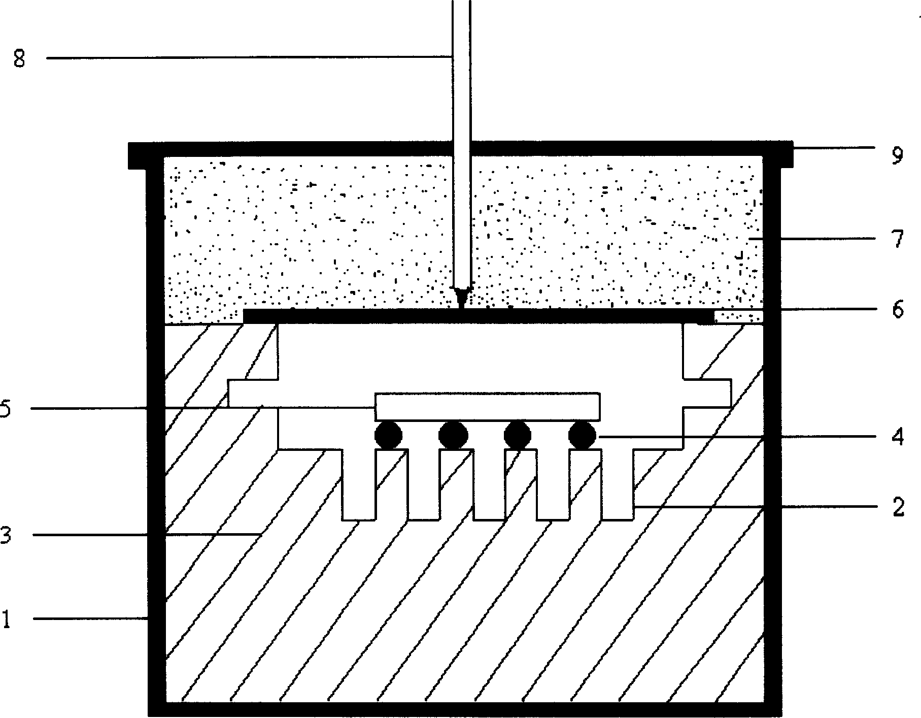
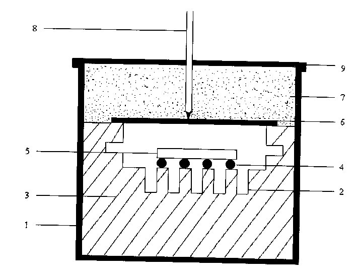
[0024] Vapor transport equilibrium (VTE) technology used in the present invention prepares composite substrate material MgIn 2 o 4 / MgO experimental setup schematic diagram see figure 1 , in the platinum crucible 1, a certain ratio of MgIn with pores 2 is placed 2 o 4 and In 2 o 3 Mixed material block 3, the upper part of the material block 3 is platinum wire 4, the double-sided polished or single-sided polished MgO wafer 5 is placed on the platinum wire 4, and the upper part of the material block 3 has platinum sheet 6 and MgIn 2 o 4 and In 2 o 3 The mixed powder 7 is covered, the thermocouple 8 is inserted into the powder 7, and the top of the crucible 1 is sealed with a platinum cover 9.

[0025] Vapor transport equilibrium (VTE) technology is a mass transport process, so there should be enough In in the crucible 2 o 3 supply, and secondly, the equilibrium of the gas phase is dependent on In 2 o 3 A steady stream from MgIn 2 o 4 and In 2 o 3 It is maintained...


PUM


Abstract

A compound substrate material suitable for InN-GaN epitaxial growth is to set a layer of MgIn2O4 o MgO single crystal. The preparation method is to put mixed ingots of MgIn2O4 and In2o3 with gas holes in a Pt pot, put or hang a MgO wafer of double or single polish on Pt silk added by a Pt plates covered by mixed powders of MgIn2O4 and In2O3 and cover the pot closely by a Pt cover then put it in a resistance furnace, heating up to 800~1400deg.c. kept constant for 20~100h, the In2O3 is reacted with MgO in solid phase by In3+ ionic diffusion to get the said material.

Description

technical field [0001] The invention relates to InN-GaN epitaxial growth, in particular to a composite substrate material suitable for InN-GaN epitaxial growth and a preparation method thereof. Background technique [0002] Group III nitride semiconductor material InN-GaN has excellent characteristics, such as stable physical and chemical properties, high thermal conductivity and high electron saturation velocity, and the optical transition probability of direct bandgap materials is an order of magnitude higher than that of indirect bandgap materials. Therefore, broadband Gap InN-GaN-based semiconductors show promising applications in short-wavelength light-emitting diodes, lasers, and UV detectors, as well as high-temperature electronic devices. Due to the relatively high melting point of InN-GaN, N 2 It is very difficult to prepare InN-GaN bulk single crystal with high saturated vapor pressure, so InN-GaN is generally grown on a heterogeneous substrate by epitaxial techno...

Claims


Application Information

Patent Timeline
IPC IPC(8): H01L21/08
Inventor 周圣明徐军王海丽杨卫桥李抒智彭观良周国清宋词杭寅蒋成勇赵广军司继良
Owner SHANGHAI INST OF OPTICS & FINE MECHANICS CHINESE ACAD OF SCI
Why Eureka
Try Eureka