


Quick Research
Generate reliable direction feasibility study reports for your R&D in just a few steps.

Technical Q&A
Discover and master advanced knowledge NOW. Basics, ideas, possibilities, all at once.

Find Solutions
As an expert in R&D theories, this can generate solutions to your technical problems instantly.

Evaluate Feasibility
Analyze your overall solution with one click, know your potential R&D risks in advance.

Monitor Landscape
Get weekly tech updates, stay abreast of the latest tech innovations and key insights.
Semiconductor memory
A memory and semiconductor technology, which is applied in semiconductor devices, static memory, semiconductor/solid-state device manufacturing, etc., can solve the problems of chip size chip cost increase, etc., and achieve the effect of avoiding defects and minimizing layout area
- Summary
- Abstract
- Description
- Claims
- Application Information
AI Technical Summary
Problems solved by technology
Method used
Image

Examples
Embodiment Construction
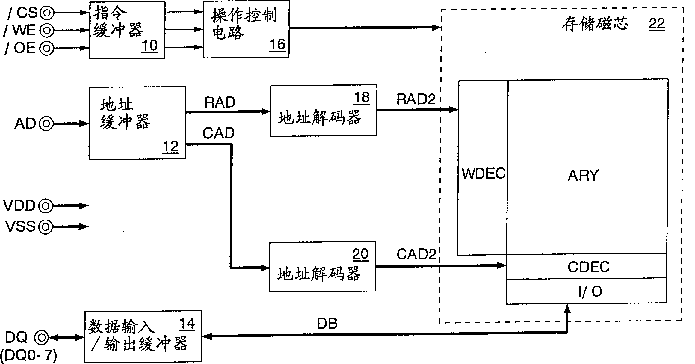
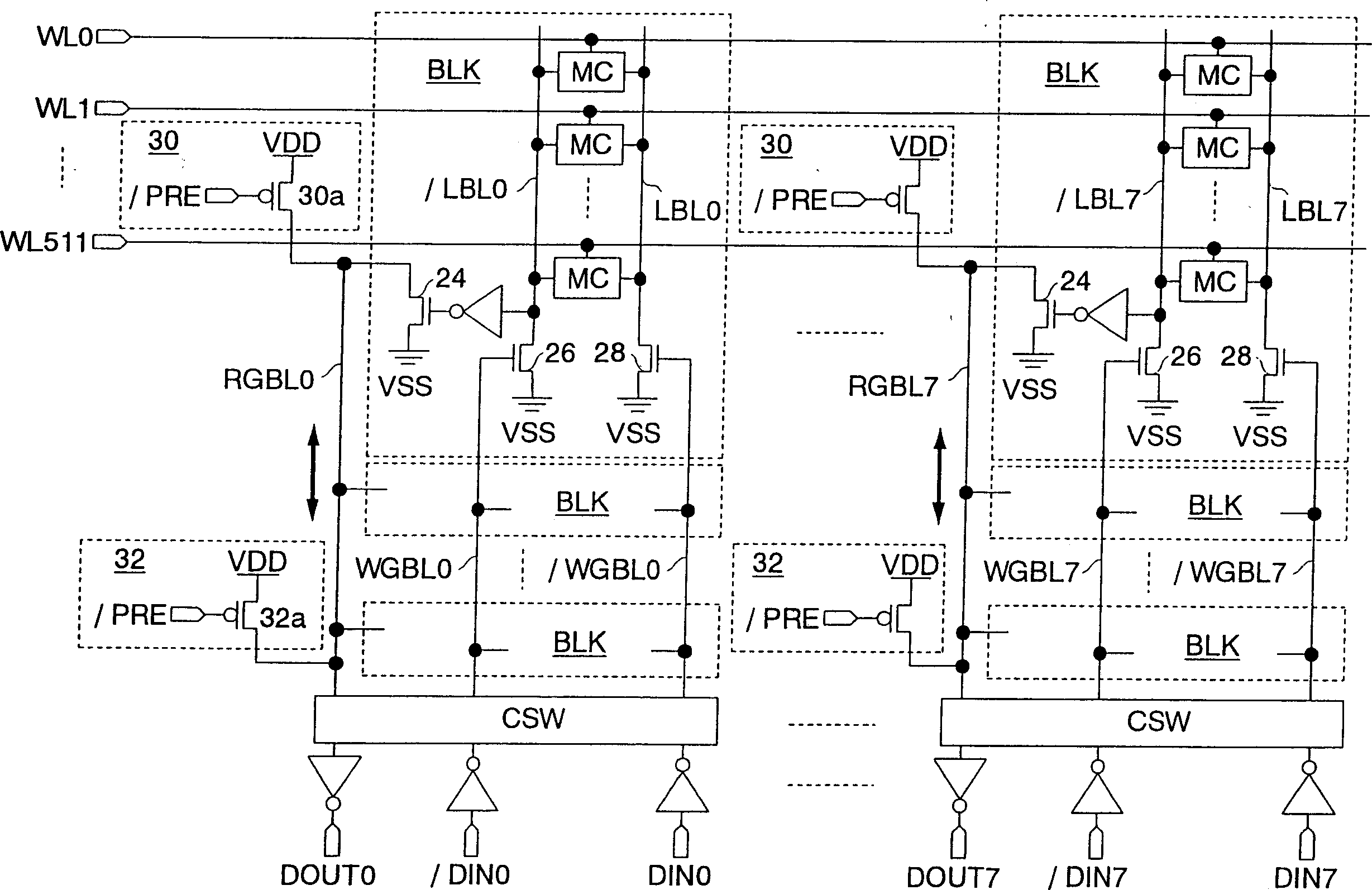
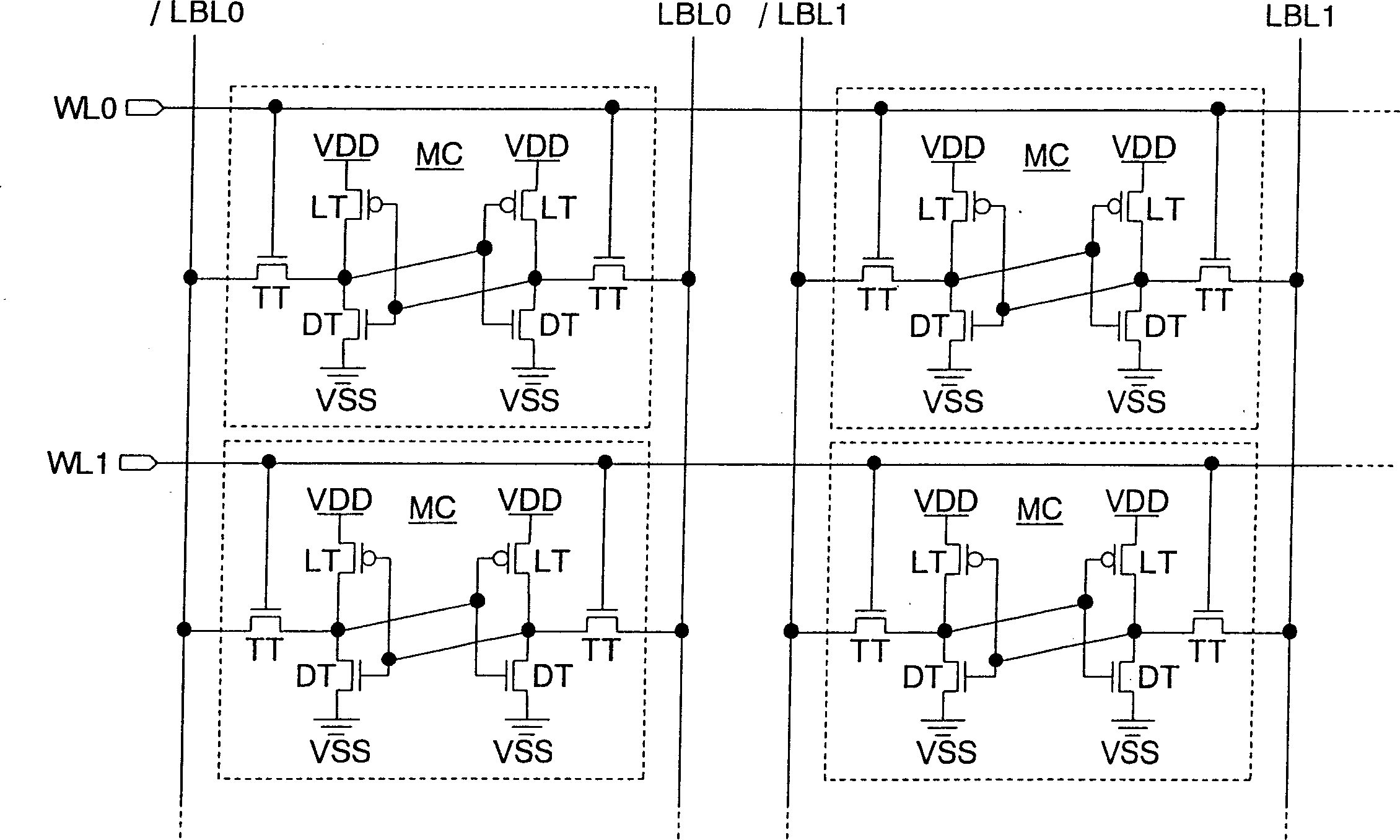
[0030] Embodiments of the present invention will be described below with reference to the accompanying drawings. In the drawings, each thick line represents a signal line composed of a plurality of lines. Signals preceded by " / " are negative logic. Double circles in the figure indicate external terminals. In the following description, the signal name may be abbreviated, such as " / CS signal" means "chip select signal".
[0031] figure 1 A first embodiment of the semiconductor memory of the present invention is shown. This semiconductor memory is formed as an SRAM on a silicon substrate by using a CMOS process.
[0032]This SRAM has an instruction buffer 10 , an address buffer 12 , a data input / output buffer 14 , an operation control circuit 16 , address decoders 18 and 20 , and a memory core 22 .
[0033] The command buffer 10 receives command signals (chip select signal / CS, write enable signal / WE, and output enable signal / OE) from the outside. The address buffer 12 re...
PUM
 Abstract
Description
Claims
Application Information
 - R&D Engineer
- R&D Manager
- IP Professional
- Industry Leading Data Capabilities
- Powerful AI technology
- Patent DNA Extraction
Browse by: Latest US Patents, China's latest patents, Technical Efficacy Thesaurus, Application Domain, Technology Topic, Popular Technical Reports.
© 2024 PatSnap. All rights reserved.Legal|Privacy policy|Modern Slavery Act Transparency Statement|Sitemap|About US| Contact US: help@patsnap.com