Method for making welding pad

A manufacturing process and conductive layer technology, applied in the field of making self-aligned pads, which can solve problems such as short circuits and out-diffusion of copper atoms

Inactive Publication Date: 2003-12-31
UNITED MICROELECTRONICS CORP
View PDF1 Cites 8 Cited by
  • Summary
  • Abstract
  • Description
  • Claims
  • Application Information

AI Technical Summary

Problems solved by technology

However, the edge portion (edge ​​portion) 26 of the welding pad 16 produced in the prior art, because copper is in direct contact with the sheath layer 18, often has the phenomenon of outward diffusion of copper atoms (outdiffusion), thereby causing a short circuit (short circuit). )

Method used


Image

  • Method for making welding pad
  • Method for making welding pad
  • Method for making welding pad

Examples


Embodiment Construction

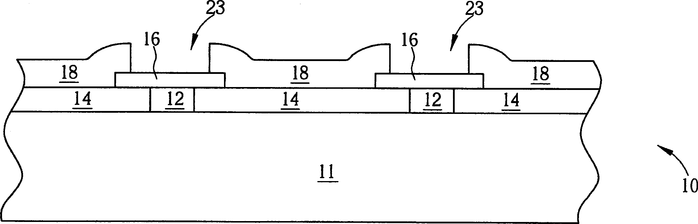
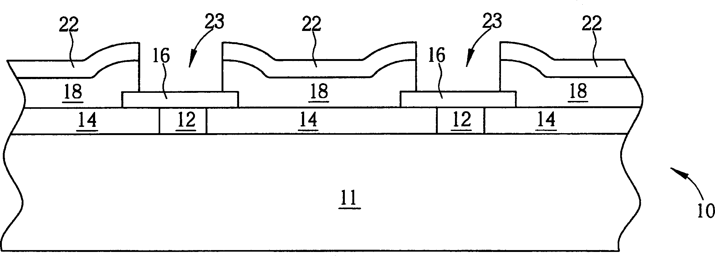
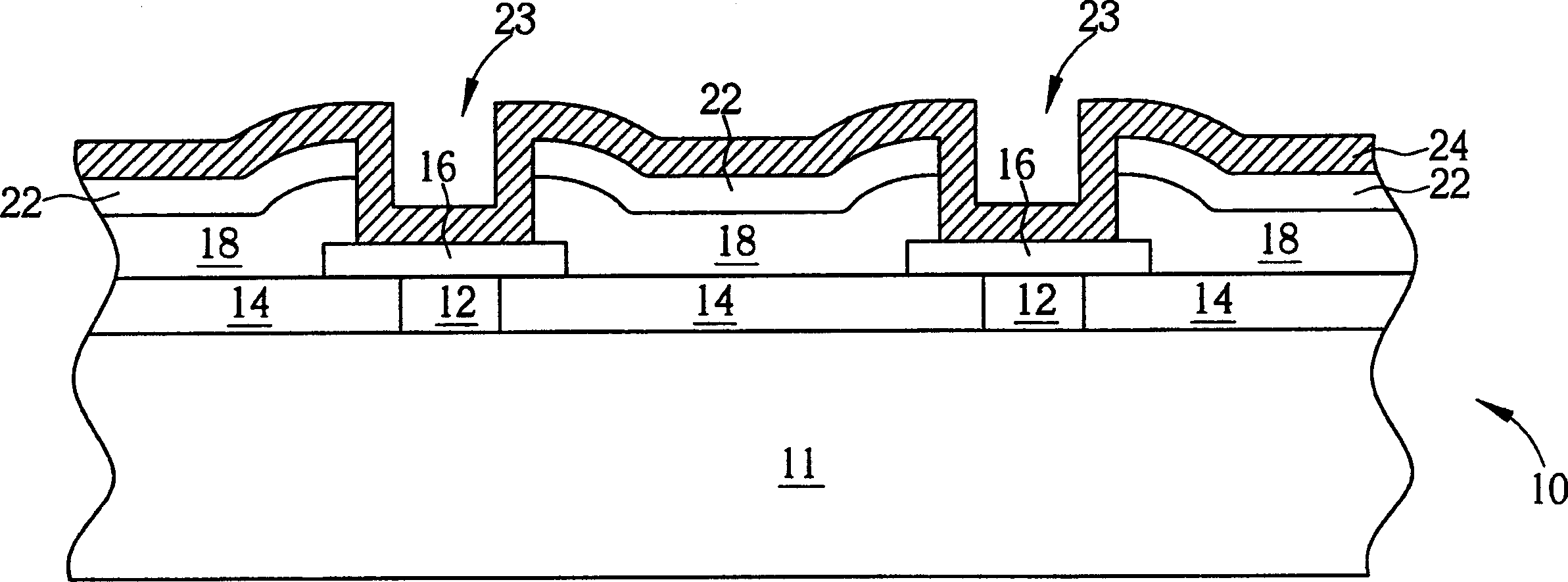
[0015] see Figure 5 to Figure 8 , Figure 5 to Figure 8 It is a schematic diagram of a method for fabricating a self-align bonding pad 109 on a semiconductor wafer according to the first embodiment of the present invention. Such as Figure 5As shown, the present invention first forms at least one conductive object 102 on the silicon substrate 101 of a semiconductor wafer 100, and the conductive object 102 may be a conductive plug, a wire (metal line), a metal interconnection ( metal interconnection) or a pair of damascene structure (dual damascence structure) conductor. Each conductive object 102 is disposed in a first dielectric layer 104 to be electrically isolated effectively, and the material constituting the conductive object 102 includes tungsten (tungsten, W), copper (copper), aluminum (aluminum), aluminum copper alloy (aluminum-copper-alloy), or other conductive materials.

[0016] and Figure 5 A conductive plug is used for illustration. First, at least one meta...


PUM


Abstract

The invention provides a process for making welding pad on a substrate, the substrate includes a first dielectric layer and a first conducting layer, first forming a second conductive layer on the substrate surface, then proceeding a heat treatment process, to form a third conductive layer in the first and second conductive layer, at the same time oxygenizing completely the residual second conductive layer to form a second dielectric layer, lastly forming a third dielectric layer, and removing each of the dielectric layer above the first conductive layer.

Description

technical field [0001] The invention relates to a method for making a bonding pad, in particular to a method for making a self-aligning pad by using an alloy process and a photo-etching-process (PEP). The method of quasi-welding pad (self align bonding pad). Background technique [0002] In the structure of integrated circuits, when each transistor (transistor) or memory unit (cell) is completed, it must first be electrically connected to metal lines (metal lines) located in different metal layers, and then connected via each metal line. After the packaging is completed, the integrated circuit can be electrically connected to terminals through the pads and then electrically connected to external circuits. In the early days of integrated circuit development, Al-metal-SiO2 dielectric material has been the standard material used in metal interconnect design in the industry. Such a combination of materials has always been popular due to the support of m...

Claims


Application Information

Patent Timeline
IPC IPC(8): H01L21/28H01L21/44H01L21/768
Inventor 李秋德
Owner UNITED MICROELECTRONICS CORP
Why Eureka
Try Eureka