Method of reducing microparticle residue and defect

A technology of manufacturing method and rinsing method, which is applied in the direction of electrical components, semiconductor/solid-state device manufacturing, circuits, etc., and can solve the problems of changing the overall dielectric properties of the ONO dielectric layer 30 and prolonging the soaking time

Inactive Publication Date: 2003-12-03
MACRONIX INT CO LTD
View PDF0 Cites 1 Cited by
  • Summary
  • Abstract
  • Description
  • Claims
  • Application Information

AI Technical Summary

Problems solved by technology

However, when performing this cleaning process, if these polymer particles and ONO barriers are to be completely removed, the soaking time must be prolonged, so that the cleaning solution will affect the top oxide layer (top) in the ONO dielectric layer 30 oxide) causes corrosion (less than 60 angstroms), and the overall dielectric properties of the ONO dielectric layer 30 are changed

Method used


Image

  • Method of reducing microparticle residue and defect
  • Method of reducing microparticle residue and defect
  • Method of reducing microparticle residue and defect

Examples


Embodiment Construction

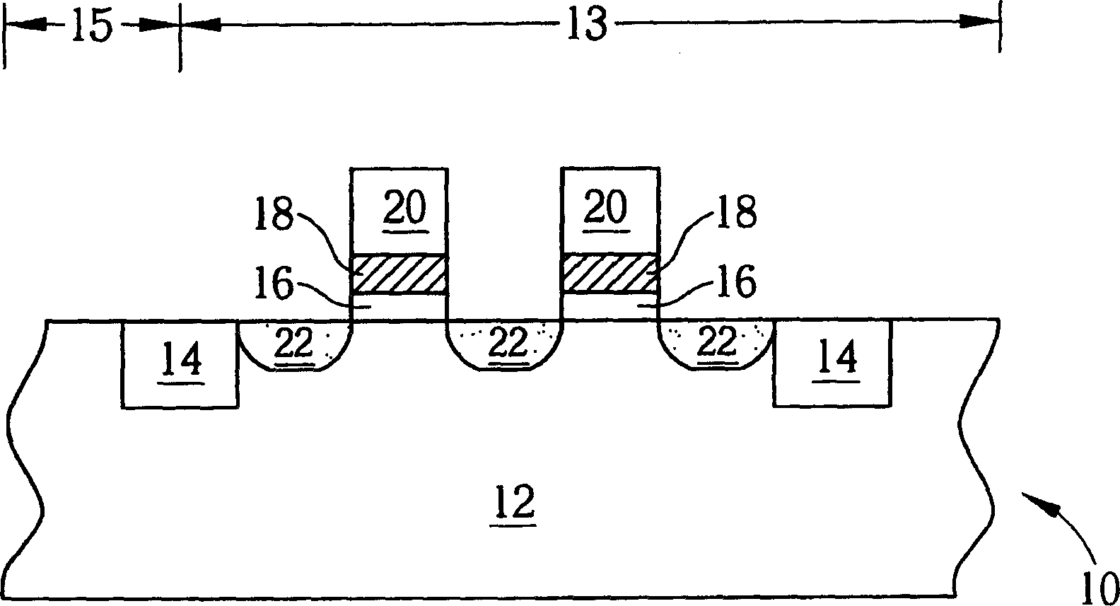
[0030] Please refer to Figure 6 to Figure 12 , Figure 6 to Figure 12 It is a schematic diagram of the method for making a semiconductor chip with an ONO structure according to the present invention. Such as Image 6 As shown, a semiconductor chip 50 includes a silicon substrate 52, wherein the silicon substrate 52 includes an N-type well 56, and a P-type well 58 located in the N-type well 56, and another buffer oxide layer 54 is located on the substrate 52 , and the semiconductor chip 50 is divided into a first area 60 intended to form a memory array area (array area) and a second area 62 intended to form a peripheral area (peripheral area) by a shallow trench isolation area 57 .

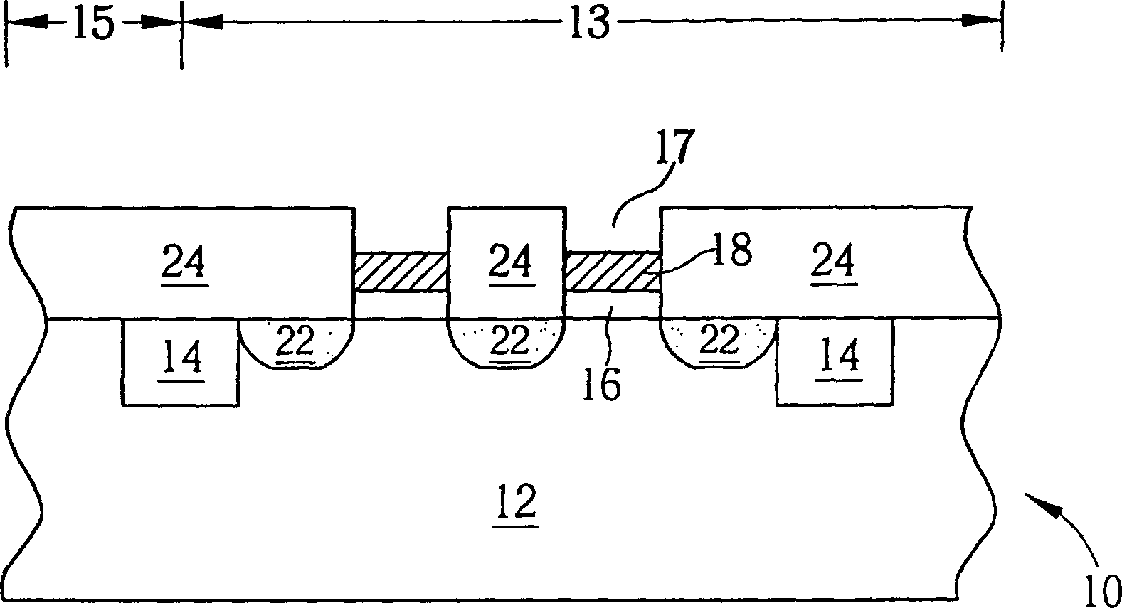
[0031] Such as Figure 7 As shown, a chemical vapor deposition (CVD) process is then performed to sequentially form a polysilicon layer 64 and a silicon nitride layer 66 covering the buffer oxide layer 54 . In a preferred embodiment of the present invention, polysilicon layer 64 has a thicknes...


PUM

PropertyMeasurementUnit
Thicknessaaaaaaaaaa
Thicknessaaaaaaaaaa

Abstract

A process for decreasing the residual microparticles and defects includes providing a semiconduct chip containing the first area covered by a oxide-nitride-oxide (ONO) layer and the second area covered by the second and the first polysilicon layers, an oxide layer, and said ONO layer, generating a photoresist layer on ONO layer to cover the first area, dry etching on said ONO layer and two polysilicon layers in the second area, removing the photoresist layer, flushing with a buffer oxide layer etching liquid for removing oxide layer, and flushing with SC-1 solution and then with SC-2 solution.

Description

technical field [0001] The invention relates to a method for manufacturing a semiconductor element with an oxide-nitride-oxide (ONO) layer, in particular to a method for manufacturing a flash memory including cascade flushing. Background technique [0002] Flash memory (flash memory) has the characteristics of small size and no need for current for keeping data, so it is often used in portable electronic products, such as mobile phones or IC cards. When making flash memory, an array area (array area) will be set on the semiconductor chip to make millions of flash memory cells (flash memory cells), and a peripheral area (peripheral area) for To make a peripheral circuit (peripheral circuit) to control the reading, writing and erasing of the memory cells in the array area. [0003] The memory cell includes a pass transistor, usually a metal-oxide-semiconductor transistor (MOS), and a storage capacitor. The design of the storage capacitor element inclu...

Claims


Application Information

Patent Timeline
IPC IPC(8): H01L21/302H01L21/822H01L21/8239
Inventor 黄文信张国华
Owner MACRONIX INT CO LTD
Why Eureka
Try Eureka