Mfg. appts. of electronic device, mfg. method of electronic device and mfg. program of electronic device

A technology for electronic devices and manufacturing devices, which is applied to the assembly of printed circuits with electrical components, semiconductor/solid-state device manufacturing, and electrical solid-state devices. Changes, shortening of production cycle time, and the effect of preventing quality deterioration

Inactive Publication Date: 2003-10-08
SEIKO EPSON CORP
View PDF0 Cites 0 Cited by
  • Summary
  • Abstract
  • Description
  • Claims
  • Application Information

AI Technical Summary

Problems solved by technology

Then, when the line is stopped for a certain period of time or longer, it is difficult to avoid damage to the product because the product under heat treatment cannot be retracted.
[0010] In addition, since the heat is also transferred to the next carrier substrate 801 to be heat-treated before the heater section 811, it is difficult to perform product quality control.
[0011] In addition, when the assembly line recovers from a stop, preheating, peak heating, and cooling are performed again. Since the damaged product part needs to be sent out of the reflow soldering process, the switch of the heat source of the machine is turned on, so there is a delay after recovery. The problem of increased waiting time for normal operation of heat treatment and cooling treatment
[0012] In addition, in the cooling zone 814 of the reflow soldering process, due to the use of low-temperature air cooling, the cooling treatment time is increased, especially for lead-free solder paste, it is very difficult to prevent thermal oxidation

Method used


Image

  • Mfg. appts. of electronic device, mfg. method of electronic device and mfg. program of electronic device
  • Mfg. appts. of electronic device, mfg. method of electronic device and mfg. program of electronic device
  • Mfg. appts. of electronic device, mfg. method of electronic device and mfg. program of electronic device

Examples


Embodiment Construction

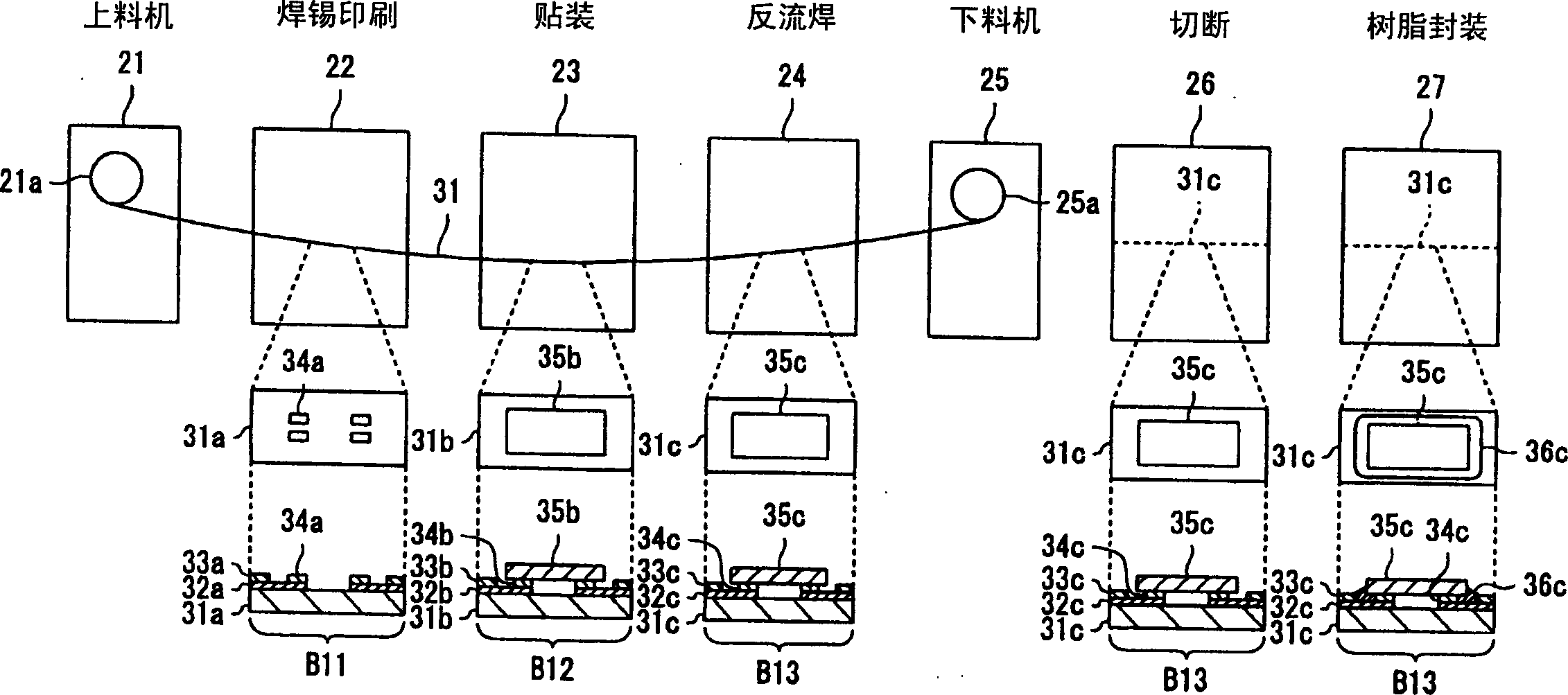
[0132] Hereinafter, an electronic device manufacturing apparatus and a manufacturing method thereof according to an embodiment of the present invention will be described with reference to the drawings.

[0133] figure 1 A method of manufacturing an electronic device according to a first embodiment of the present invention is shown.

[0134] exist figure 1 Among them, a solder coating section 22 , a mounting section 23 and a reflow soldering section 24 are arranged side by side between the loader 21 and the unloader 25 along the transport direction of the tape carrier substrate 31 .

[0135] On the other hand, on the tape carrier board 31 , electronic component mounting regions are provided on the respective circuit blocks B11 to B13 , and circuit boards 31 a to 31 c are provided on the respective circuit blocks B11 to B13 . Then, wirings 32a to 32c are formed on the respective circuit boards 31a to 31c, and insulating films 33a to 33c are formed on the respective wirings 3...


PUM


Abstract

Quality control of product manufacturing is performed with a simple structure and, in addition, damage of a product when a production line is stopped is avoided. A preheating block approaches a circuit substrate having a predetermined length along a tape substrate from a predetermined position by gradual upward movements to carry out preheating and is then returned to the predetermined position, a main heating block arranged close to the preheating block is made to contact the circuit substrate on which the preheating has been carried out and which is transported in a predetermined tact to apply peak heating and is then restored to the predetermined position, and a cooling block accesses the circuit substrate to which the peak heating has been applied to cool the circuit substrate and is then returned to the predetermined position.

Description

technical field [0001] The invention relates to an electronic device manufacturing device, a manufacturing method of the electronic device and a manufacturing program of the electronic device, and is especially suitable for the solder reflow soldering process of a carrier tape substrate installed with electronic components. Background technique [0002] In semiconductor manufacturing equipment, there is a process of bonding a semiconductor chip by, for example, reflow soldering in a COF (Chip On Film) module and a TAP (Tape Automated Bonding) module. [0003] Figure 17 A prior art method of manufacturing an electronic device is shown. [0004] exist Figure 17 Among them, in the reflow soldering process, heater sections 811 to 813 and a cooling section 814 are provided along the conveying direction of the right arrow of the tape carrier substrate 801 . Here, in the reflow soldering process, if rapid high-temperature heating is performed, reflow cracks may occur in the conn...

Claims


Application Information

Patent Timeline
Patent Type & Authority Applications(China)
IPC IPC(8): H01L21/60B23K1/008B23K3/08H01L21/00H05K1/18H05K3/34
CPCH01L2924/0002H01L21/67109B23K1/008H05K2203/1545B23K3/085H05K1/189H05K3/3494B23K2201/40B23K2101/40H01L2924/00H01L21/60
Inventor 塩泽雅邦
Owner SEIKO EPSON CORP
Why Eureka
Try Eureka