


Quick Research
Generate reliable direction feasibility study reports for your R&D in just a few steps.

Technical Q&A
Discover and master advanced knowledge NOW. Basics, ideas, possibilities, all at once.

Find Solutions
As an expert in R&D theories, this can generate solutions to your technical problems instantly.

Evaluate Feasibility
Analyze your overall solution with one click, know your potential R&D risks in advance.

Monitor Landscape
Get weekly tech updates, stay abreast of the latest tech innovations and key insights.
Ceramic parts formed micro crowning on its surface and its mfg. method
A manufacturing method, ceramic technology, applied in semiconductor/solid-state device manufacturing, electrical components, gaseous chemical plating, etc., can solve problems such as broken, reduced mechanical strength of ceramic parts, and reduced mechanical strength
- Summary
- Abstract
- Description
- Claims
- Application Information
AI Technical Summary
Problems solved by technology
Method used
Image

Examples
Embodiment 1
[0074] *Δ: small effect, ○: large effect.
[0075] When observing and evaluating the surface of the above-mentioned etched alumina ceramic plate with an electron microscope, under the conditions of the present invention, on the surface of the crystal particles constituting the surface of the ceramic substrate, there are a plurality of protruding portions smaller than the crystal particles. of ceramics.
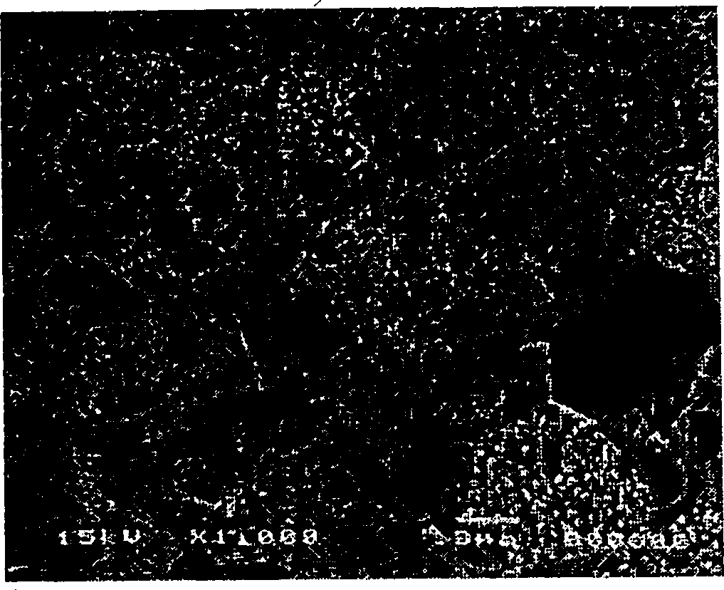
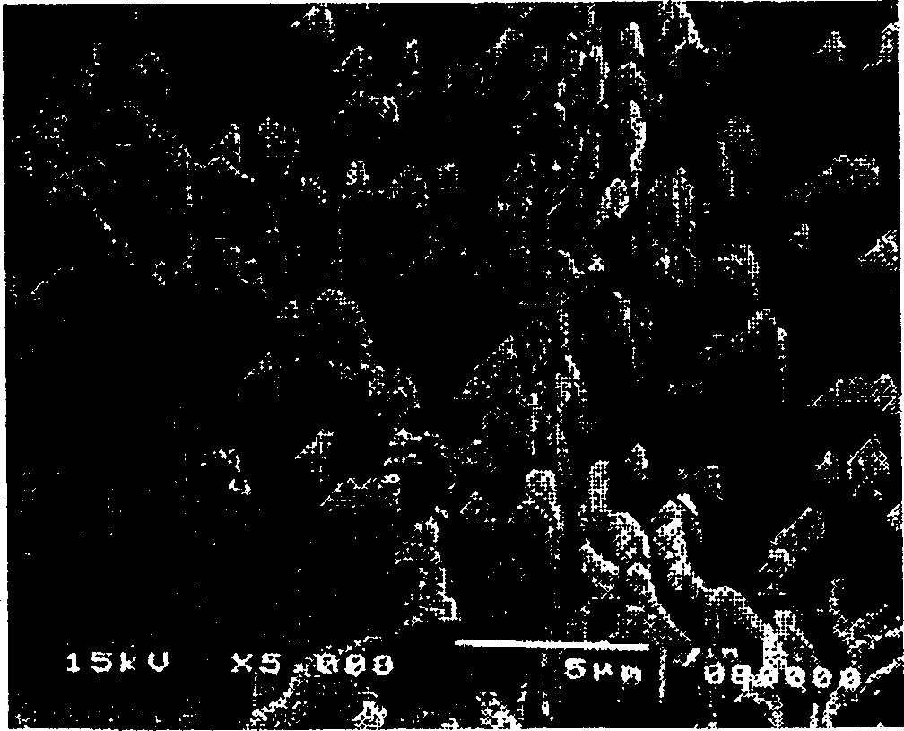
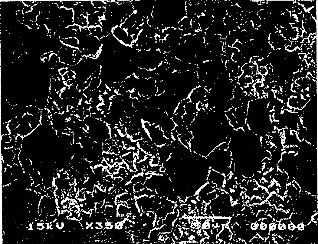
[0076] The electron microscope photographs, such as figure 1 , figure 2 , image 3 and Figure 4 shown. figure 1 and figure 2 It is the case where the surface of alumina ceramics whose surface is ground is treated at an etching solution temperature of 230°C and a pressure of 1 MPa, figure 1 It is a photo taken at 1000 times magnification, figure 2 This is a photo taken at 5000x magnification. image 3 and Figure 4 It is the case where the alumina ceramics with a sintered surface are treated at an etching solution temperature of 230°C and a pressure of 1M...
Embodiment 2
[0097] Alumina ceramic plates with a purity of 99.7% by weight, a bulk density of 3.97g / cm3, and an average particle size of 40 microns were used. On the other hand, an aqueous sulfuric acid solution with a sulfuric acid concentration of 25% by weight was used as an acidic etching solution. Next, immerse the alumina ceramic plate in an acidic etchant, perform an etching treatment for a given period of time, and perform an etching process on the surface layer (within about 80 microns) with a diameter of 0.5 to 10 times the average particle diameter and a large diameter in the depth direction. Concave-convex structure of some micropores. During this etching process, as shown in Table 1, the acidic etching solution was kept at 25 to 230° C., and a pressure of 0.1 to 10 MPa was applied to the acidic etching solution, and the etching time was set in consideration of the holding temperature and pressure of the etching solution.
[0098] Etching solution temperature
(℃) ...
Embodiment 3
[0105] A yttrium aluminum garnet plate with a purity of 97% by weight, a bulk density of 4.32g / cm3, and an average particle size of 5 microns was used. On the other hand, an aqueous sulfuric acid solution with a sulfuric acid concentration of 25% by weight was used as an acidic etching solution. Next, immerse the yttrium aluminum garnet plate in an acidic etching solution at a temperature of 230°C for 3 hours of etching treatment, and carry out an etching process on the surface layer (within about 80 microns) containing a diameter 0.5 to 10 times the average particle size, Concave-convex structuring of micropores with large diameter portions in the depth direction. Figure 7 and Figure 8 The surface layer of the above-mentioned yttrium aluminum garnet plate having a concavo-convex structure including micropores with large-diameter portions in the depth direction is shown planarly at different magnifications. Figure 9 The state (shape) in the concavo-convex structure is furt...
PUM
| Property | Measurement | Unit |
|---|---|---|
| particle size | aaaaa | aaaaa |
| thickness | aaaaa | aaaaa |
| particle size | aaaaa | aaaaa |
Abstract
Description
Claims
Application Information
 - R&D Engineer
- R&D Manager
- IP Professional
- Industry Leading Data Capabilities
- Powerful AI technology
- Patent DNA Extraction
Browse by: Latest US Patents, China's latest patents, Technical Efficacy Thesaurus, Application Domain, Technology Topic, Popular Technical Reports.
© 2024 PatSnap. All rights reserved.Legal|Privacy policy|Modern Slavery Act Transparency Statement|Sitemap|About US| Contact US: help@patsnap.com