


Quick Research
Generate reliable direction feasibility study reports for your R&D in just a few steps.

Technical Q&A
Discover and master advanced knowledge NOW. Basics, ideas, possibilities, all at once.

Find Solutions
As an expert in R&D theories, this can generate solutions to your technical problems instantly.

Evaluate Feasibility
Analyze your overall solution with one click, know your potential R&D risks in advance.

Monitor Landscape
Get weekly tech updates, stay abreast of the latest tech innovations and key insights.
Circuit base board and method for mfg. same
A technology of circuit substrate and manufacturing method, which is applied in the direction of printed circuit manufacturing, circuit substrate material, multi-layer circuit manufacturing, etc., can solve the problems of insufficient conductor connection, uneven thickness, uneven density, etc., and achieve high-density wiring discrete sexual effect
- Summary
- Abstract
- Description
- Claims
- Application Information
AI Technical Summary
Problems solved by technology
Method used
Image

Examples
Embodiment 1
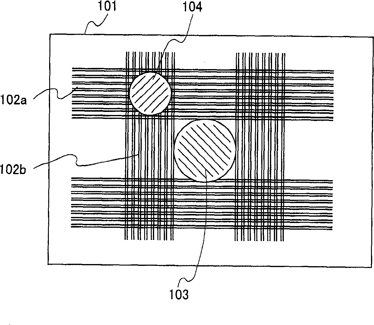
[0074] figure 1 is a schematic plan view of the circuit board of the first embodiment. In this embodiment, a case where a glass epoxy substrate is used as an insulator layer including reinforcing material sheets 101 having a density distribution in the planar direction will be described. exist figure 1 In the figure, for the sake of explanation, the weft yarn 102a and the warp yarn 102b of the glass woven cloth inside the base material are shown in the figure. The cross-sectional area of the inner passage 103 provided outside the overlappingly woven portion of the glass fiber (the portion with high density of the reinforcing material sheet) is larger than that of the inner passage provided at the overlappingly woven portion (the portion with high density of the reinforcing material sheet) 104 has a large cross-sectional area. In the above, the ratio of the cross-sectional area of the passage is preferably 1.15 times or more, more preferably 1.4 times, between the overla...
Embodiment 2
[0099] Image 6 It is a cross-sectional schematic diagram of the multilayer circuit board of the second embodiment of the present invention. The multilayer substrate of this embodiment has a structure in which the circuit substrate described in Embodiment 1 is laminated on at least one side of a core substrate made of a compressible insulating base material. In the figure, double-sided substrates 401 made of aramid epoxy material are used as the core substrate, and circuit boards 402 made of glass epoxy material having the structure described in the first embodiment are laminated on both sides of the core substrate. side structure.
[0100] The multilayer circuit board of this example can be manufactured as follows.
[0101] First, a double-sided circuit board was produced using an aramid epoxy prepreg. Regarding the production method of the double-sided circuit board, firstly, cover films are temporarily crimped on both surfaces of an aramid epoxy prepreg to form through h...
Embodiment 3
[0107] Figure 7 It is a cross-sectional schematic diagram of the multilayer substrate of the third embodiment of the present invention. The multilayer substrate of this embodiment has the circuit substrate 501 of the first or second embodiment as a core substrate, and a circuit substrate 502 in which an insulator layer thinner than the insulator layer of the core substrate is laminated on at least one side of the core substrate . Finer internal vias can be formed with low resistance on thin insulator layers. This is because, even with the same hole diameter, if the length of the inner via is reduced, that is, the thickness of the insulator layer is reduced, the connection resistance is reduced.
[0108] The case where the four-layer multilayer substrate of Example 2 is used as the core substrate and the polyimide film is used as the insulator layer thinner than the insulator layer of the core substrate will be described.
[0109] The multilayer substrate of this embodiment...
PUM
 Abstract
Description
Claims
Application Information
 - R&D Engineer
- R&D Manager
- IP Professional
- Industry Leading Data Capabilities
- Powerful AI technology
- Patent DNA Extraction
Browse by: Latest US Patents, China's latest patents, Technical Efficacy Thesaurus, Application Domain, Technology Topic, Popular Technical Reports.
© 2024 PatSnap. All rights reserved.Legal|Privacy policy|Modern Slavery Act Transparency Statement|Sitemap|About US| Contact US: help@patsnap.com