Semiconductor device with shallow-channel isolation structure and its preparing process
A semiconductor, shallow trench technology, applied in the fields of semiconductor/solid-state device manufacturing, semiconductor devices, electric solid-state devices, etc., can solve the problems of difficult to maintain P-FET characteristics, difficult to maintain device characteristics at the same time, etc.
- Summary
- Abstract
- Description
- Claims
- Application Information
AI Technical Summary
Problems solved by technology
Method used
Image
Examples
Embodiment 1
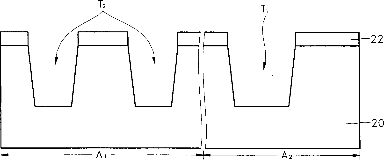
[0034] First, refer to Figure 3A , a masking pattern 22 is formed on the semiconductor substrate 20 to expose a region for device isolation. The semiconductor substrate 20 containing predetermined impurities is defined as an element region in which a memory device will be formed and a core region in which a P-FET will be formed, and a peripheral region. exist Figure 3A In , the element area A1 and the core and peripheral area A2 are shown. Masked pattern 22 may be formed of a material that has a very low etch selectivity relative to silicon and is resistant to oxidation. For example, masked pattern 22 may be a stack of silicon oxide and silicon nitride layers.
[0035] Then, using the masked pattern 22 as a mask, the semiconductor substrate 20 is dry etched to a predetermined depth. As a result, a first trench T1 and a second trench T2 are formed in the semiconductor substrate 20 . Here, the first and second trenches T1 and T2 are shallow trenches for forming shallow tr...
Embodiment 2
[0045] The second preferred embodiment of the present invention is the same as the first embodiment described above from the process of forming the trenches T1 and T2 to the process of forming the thermal oxide layer 24 . Therefore, only the processes after forming the thermal oxide layer 24 will be described.
[0046] First, refer to Figure 5A , and form a photoresist pattern 26 through a photolithography process to expose the element region A1. Thereafter, the thermal oxide layer 24 in the exposed element region A1 is etched by isotropic etching. At this time, the thermal oxide layer 24 is etched to leave a predetermined thickness in the second trench T2. The silicon semiconductor substrate 20 is hydrophobic and thus easily damaged by isotropic etching. Thus, a thermal oxide layer 24 remains to prevent such damage. Here, reference numeral 24a denotes a thermal oxide layer etched to a predetermined thickness.
[0047] Thereafter, if Figure 5B As shown, the photoresist...
Embodiment 3
[0051] Up to the process of forming trenches T1 and T2, the third preferred embodiment is the same as the first embodiment. Therefore, only the processes after forming the trenches T1 and T2 will be described.
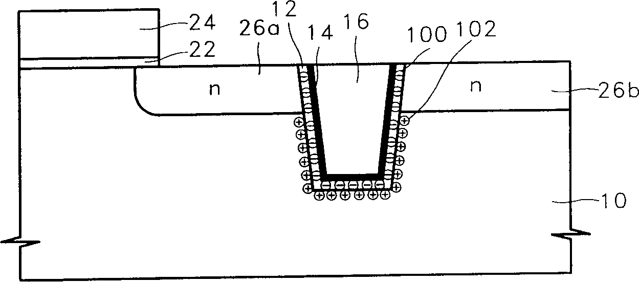
[0052] refer to Figure 6A , the first sidewall oxide layer 40 is formed by thermally oxidizing the inner surfaces of the trenches T1 and T2. At this time, the first sidewall oxide layer 40 is formed with a thickness capable of preventing sustain current from being generated in the P-FET in the core region and the peripheral region A2. That is, the first sidewall oxide layer 40 should be formed with a thickness capable of preventing electrons trapped in the inner liner, which is formed by a subsequent process, from penetrating into the semiconductor substrate, for example, the thickness is 100-300 Å.
[0053] Then, if Figure 6BAs shown, a photoresist pattern 26 is formed by a known photolithography process to mask the core and peripheral area A2. Thereafter, the f...
PUM
 Abstract
Description
Claims
Application Information
 - Generate Ideas
- Intellectual Property
- Life Sciences
- Materials
- Tech Scout
- Unparalleled Data Quality
- Higher Quality Content
- 60% Fewer Hallucinations
Browse by: Latest US Patents, China's latest patents, Technical Efficacy Thesaurus, Application Domain, Technology Topic, Popular Technical Reports.
© 2025 PatSnap. All rights reserved.Legal|Privacy policy|Modern Slavery Act Transparency Statement|Sitemap|About US| Contact US: help@patsnap.com


