Semiconductive thin film inner cladding amplifying optical fiber and manufacturing method thereof
A semiconductor and inner cladding technology, applied in the field of optical fiber, can solve problems such as difficult connection, increased concentration of rare earth elements, limited bandwidth, etc., and achieve the effects of easy miniaturization, high output power, and convenient use
- Summary
- Abstract
- Description
- Claims
- Application Information
AI Technical Summary
Problems solved by technology
Method used
Image
Examples
Embodiment 1
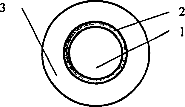
[0014] Embodiment one: see figure 1 , a nano-semiconductor film inner cladding amplifying optical fiber of the present invention is composed of three parts: a core 1, a film inner cladding 2 and an outer cladding 3. The material of the core 1 is pure silica doped with a small amount of GeO which increases the refractive index 2 Composition, the material of the inner cladding layer 2 of the film is composed of nano-semiconductor material GaAs or InP with amplifying function, and the material of the outer cladding layer 3 is pure quartz with a small amount of low refractive index additive B 2 o 3 Or fluorine (F) composition. The inner cladding layer 2 of the nano-semiconductor thin film is sandwiched between the fiber core 1 and the outer cladding layer 3 .
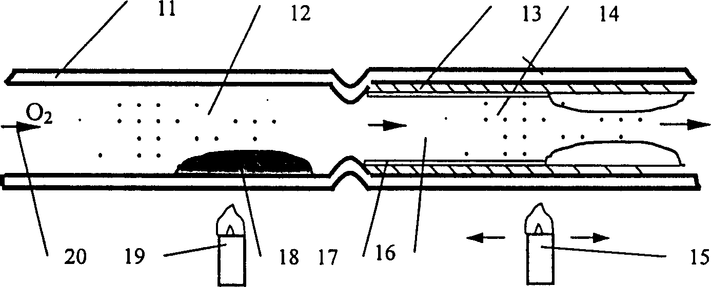
[0015] The preparation method of the amplifying optical fiber of the inner cladding layer 2 of the semiconductor thin film is as follows: first, the optical fiber preform is made by shrinking rod technology, and then the...
PUM
 Abstract
Description
Claims
Application Information
 - R&D Engineer
- R&D Manager
- IP Professional
- Industry Leading Data Capabilities
- Powerful AI technology
- Patent DNA Extraction
Browse by: Latest US Patents, China's latest patents, Technical Efficacy Thesaurus, Application Domain, Technology Topic, Popular Technical Reports.
© 2024 PatSnap. All rights reserved.Legal|Privacy policy|Modern Slavery Act Transparency Statement|Sitemap|About US| Contact US: help@patsnap.com


