
Process for preparing mask-type ROM

A technology of read-only memory and manufacturing method, which is applied in semiconductor/solid-state device manufacturing, electrical components, circuits, etc., and can solve problems that affect the initial voltage and channel opening current, and affect the accuracy of data, etc.

Inactive Publication Date: 2005-12-28
MACRONIX INT CO LTD
View PDF0 Cites 0 Cited by
  • Summary
  • Abstract
  • Description
  • Claims
  • Application Information

AI Technical Summary

Problems solved by technology

[0006] Though above-mentioned known method is often adopted, has its shortcoming to exist
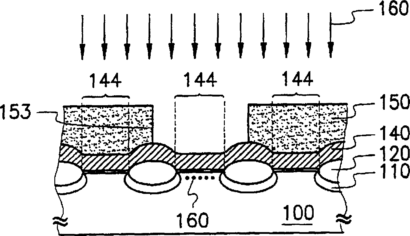
Please refer to Figure 1B Since the width of the coding window 153 of the photoresist layer 150 is greater than the width of the memory cell 144 to be implanted, the implanted ions 160 are easily diffused into the memory cell 144 that does not need to be implanted, and affect its starting voltage and channel opening current, Then affect the accuracy of data storage and retrieval

Method used


Image

  • Process for preparing mask-type ROM
  • Process for preparing mask-type ROM
  • Process for preparing mask-type ROM

Examples


Embodiment Construction

[0027] Please refer to Figures 2A-2F . Such as Figure 2A As shown, firstly, a pad oxide layer 202, a mask layer 204, and a patterned photoresist layer 206 are sequentially formed on a substrate 200, and then the photoresist layer 206 is used as a mask to remove the exposed mask layer 204 and pad oxide layer. 202. Next, ions 208 are implanted using the photoresist layer 206 as a mask to form buried bit lines 210 in the substrate 200 .

[0028] Please refer to Figure 2B , and then remove the photoresist layer 206, and then perform a thermal oxidation step to oxidize the exposed portion of the surface of the substrate 200 to form an isolation oxide layer 220, and drive the buried bit line 210 thereunder.

[0029] Please refer to Figure 2C , and then remove the mask layer 204 and the pad oxide layer 202 , and then form the gate oxide layer 230 on the substrate 200 . Then, a word line 240 perpendicular to the buried bit line 210 is formed. At this time, the part of the su...


PUM


Abstract

A manufacturing method of a mask-type read-only memory. First, a buried bit line is formed on a base, and then a gate dielectric layer and a word line are formed on the base. The word line is perpendicular to the buried bit line. At this time, the part of the substrate located between a pair of buried bit lines and below a word line serves as a memory cell. Then cover the base with a first dielectric layer, and then form several coding windows in the first dielectric layer, which are located above part of the memory cells. Then an ion is implanted into the memory unit under the encoding window, and a second dielectric layer is formed on the substrate to fill up all the encoding windows.

Description

technical field [0001] The present invention relates to a semiconductor process method (Semiconductor Process), and in particular to a mask-type read-only memory (MaskROM) manufacturing method. Background technique [0002] Among all kinds of read-only memories, the mask-type read-only memory is the simplest in structure and process. The basic structure of its memory cell (MemoryCell) is a metal oxide semiconductor transistor (MOSTransistor), and when it is programmed, it is in its gate. Ions are implanted into the channel region (Channel) below the pole (Gate) to change its threshold voltage (Threshold Voltage, VT). The mask ROM is to use the initial voltage of the storage unit to represent the data value in it, and the data value is determined by the channel opening and closing of the storage unit under a certain gate voltage when reading, and the channel’s On and off are determined by the starting voltage of the memory cell itself. [0003] Please refer to the manufactu...

Claims


Application Information

Patent Timeline
Patent Type & Authority Patents(China)
IPC IPC(8): H10B20/00
Inventor 薛正诚
Owner MACRONIX INT CO LTD
Learn More