Semiconductor structure and forming method thereof

A semiconductor and contact structure technology, used in semiconductor/solid-state device manufacturing, transistors, electrical components, etc., can solve problems such as insufficient area of ​​capacitor electrode plates, reduce limitations and difficulties, compensate for damage, and avoid collapse.

Pending Publication Date: 2022-08-09
CHANGXIN MEMORY TECH INC
View PDF0 Cites 0 Cited by
  • Summary
  • Abstract
  • Description
  • Claims
  • Application Information

AI Technical Summary

Problems solved by technology

[0004] The embodiment of the present invention provides a semiconductor structure and its forming method, which solves the problem of insufficient area of ​​the capacitor electrode plate of the semiconductor structure

Method used


Image

  • Semiconductor structure and forming method thereof
  • Semiconductor structure and forming method thereof
  • Semiconductor structure and forming method thereof

Examples


Embodiment Construction

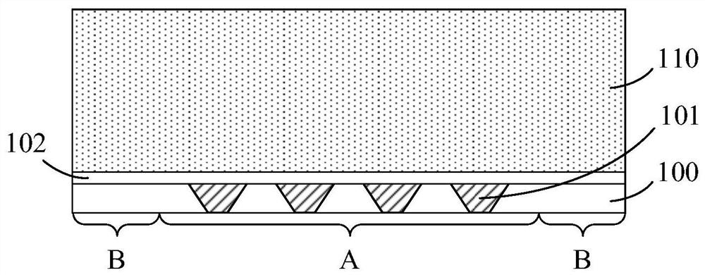
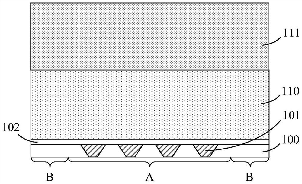
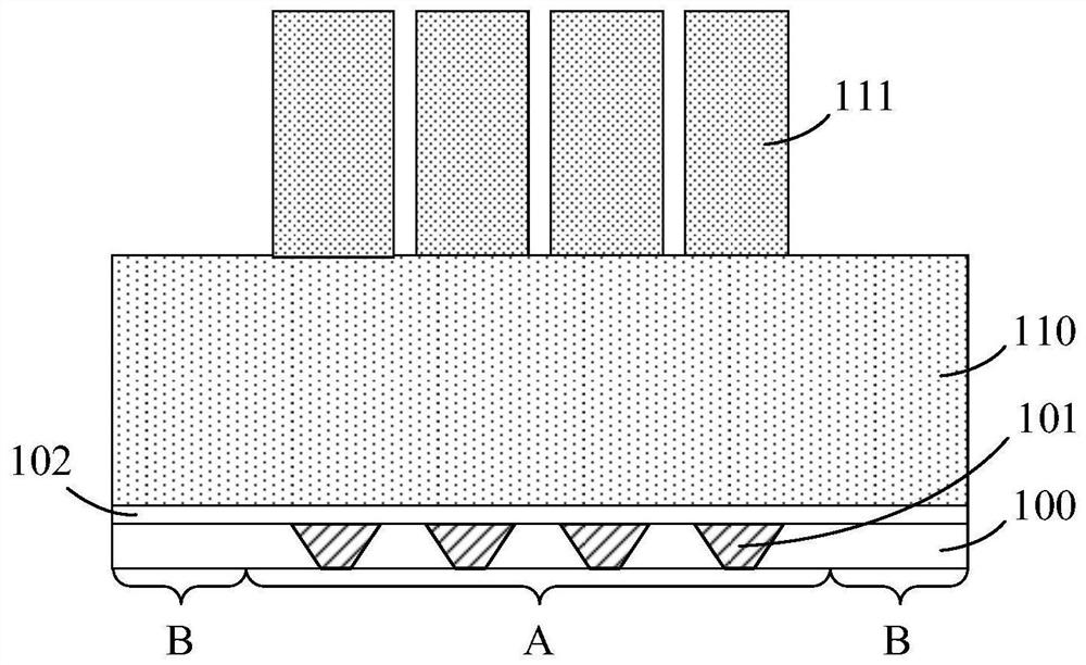
[0035] It can be known from the background art that the area of ​​the electrode plate of the semiconductor structure capacitor in the prior art is small.

[0036] The capacitor of the semiconductor structure adopts a hexagonal honeycomb layout, and the capacitor is a cylindrical or columnar structure with a very large aspect ratio. The hexagonal honeycomb layout results in that the pitch ratio of the word lines and bit lines of the semiconductor structure is fixed at Left and right, the fixed word bit line pitch ratio limits the diversity of semiconductor structure processes; when forming columnar or cylindrical capacitors with extremely large aspect ratios, in order to prevent capacitors from collapsing due to excessive aspect ratios, it is necessary to first The support layer is formed, and after the capacitor is formed, the support layer needs to be removed later. Such a formation method is complicated in process, wastes materials, and has a high process cost; because the ...


PUM

PropertyMeasurementUnit
thicknessaaaaaaaaaa
thicknessaaaaaaaaaa
thicknessaaaaaaaaaa

Abstract

The embodiment of the invention provides a semiconductor structure and a forming method thereof, and the method comprises the steps: providing a substrate and an insulating layer which are stacked, and enabling the interior of the substrate to be provided with a plurality of storage node contact structures at intervals; a latticed upper electrode layer is formed on the surface of the insulating layer, a plurality of meshes penetrating through the upper electrode layer are formed in the upper electrode layer, and the orthographic projection of each mesh on the insulating layer and the orthographic projection of one storage node contact structure on the insulating layer have an overlapping area; forming a dielectric layer on the side wall of the mesh; removing the insulating layer exposed from the meshes to expose the storage node contact structure; lower electrode layers are formed in the meshes, the lower electrode layers are located on the side, away from the upper electrode layer, of the dielectric layer and make contact with the exposed storage node contact structure, and the lower electrode layers in the different meshes are electrically insulated from one another. According to the semiconductor structure forming method provided by the embodiment of the invention, the area of the capacitor electrode plate of the semiconductor structure can be increased.

Description

technical field [0001] Embodiments of the present invention relate to the field of semiconductors, and in particular, to a semiconductor structure and a method for forming the same. Background technique [0002] Dynamic random access memory (Dynamic Random Access Memory, DRAM) is a semiconductor memory device commonly used in computers, which is composed of many repeated memory cells. Each memory cell includes a capacitor and a transistor. A large enough capacitance is the basic requirement to ensure the normal operation of the DRAM and sufficient storage retention time. In the DRAM process, the DRAM adopts a stacked capacitor structure. At present, the capacitor of the DRAM cell adopts The first is a hexagonal honeycomb layout, and the capacitors are cylindrical or columnar structures with extremely large aspect ratios. [0003] The current capacitor layout structure results in the word line to bit line pitch ratio being fixed at Left and right, the fixed word bit line p...

Claims


Application Information

Patent Timeline
Patent Type & Authority Applications(China)
IPC IPC(8): H01L21/8242H01L27/108
CPCH10B12/30H10B12/03H10B12/00
Inventor 平尔萱周震白卫平郁梦康苏星松
Owner CHANGXIN MEMORY TECH INC
Why Eureka
Try Eureka