N-polarity GaN/AlGaN-based rectifier and preparation method thereof
A rectifier and polarity technology, which is applied in the field of rectifiers, can solve the problems of reduced stability and reliability of rectifiers, difficulty in preparing N-polar GaN thin films, and reduced concentration of two-dimensional electron gas, so as to reduce threading dislocations and improve positive polarity. Improvement of conduction characteristics and quality
- Summary
- Abstract
- Description
- Claims
- Application Information
AI Technical Summary
Problems solved by technology
Method used
Image
Examples
Embodiment 1
[0040] This embodiment provides a method for preparing an N-polar GaN / AlGaN-based rectifier, including the following steps:
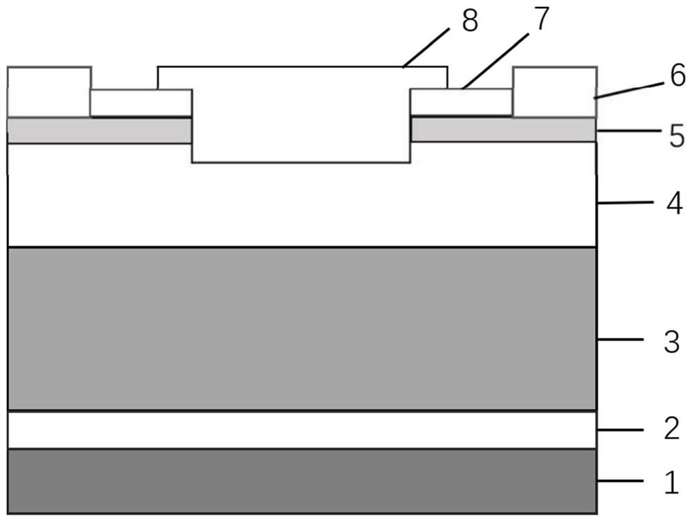
[0041] (1) If figure 1 As shown, an AlN buffer layer 2, a double SiN insertion layer structure 3, an undoped AlGaN barrier layer 4 and an undoped GaN channel layer 5 are sequentially grown on the silicon carbide substrate 1 to obtain a rectifier epitaxial wafer;
[0042] Among them, the preparation of the double SiN insertion layer structure includes sequentially growing the lower SiN insertion layer, the AlGaN buffer layer and the upper SiN insertion layer on the AlN buffer layer. The deposition time of the lower SiN insertion layer and the upper SiN insertion layer is 30-50s and 160-180s;
[0043] In order to alleviate lattice mismatch and release stress, the Al composition of the AlGaN buffer layer is larger than that in the undoped AlGaN barrier layer;
[0044] The AlN buffer layer, the AlGaN buffer layer, the undoped AlGaN barrier layer and the und...
Embodiment 2
[0060] This embodiment provides a method for preparing an N-polar GaN / AlGaN-based rectifier, which specifically includes:
[0061] (1) If figure 1 As shown, an N-polar AlN buffer layer 2 with a thickness of 160 nm, a double SiN insertion layer structure 3 with a thickness of 500 nm, a non-doped N-polar AlGaN barrier layer 4 with a thickness of 300 nm, and a thickness of 25 nm are sequentially grown on the silicon carbide substrate 1. The undoped N-polar GaN layer 5 is obtained to obtain a rectifier epitaxial wafer;
[0062] Among them, the growth process of the double SiN insertion layer structure 3 is: growing the lower SiN insertion layer 50s on the N-polar AlN buffer layer 2, growing the AlGaN buffer layer on the lower SiN insertion layer, and then growing the upper SiN insertion layer on the AlGaN buffer layer. layer 160s; wherein the Al composition of the AlGaN buffer layer is greater than that of the undoped AlGaN barrier layer;
[0063] (2) Pretreatment is carried out...
Embodiment 3
[0072] This embodiment provides a method for preparing an N-polar GaN / AlGaN-based rectifier, which specifically includes:
[0073] (1) If figure 1 As shown, a 180 nm-thick N-polar AlN buffer layer 2, a 600-nm-thick double SiN intercalation layer structure 3, a 320-nm-thick undoped N-polar AlGaN layer 4, and a 40-nm-thick non-polar AlGaN layer were sequentially grown on the silicon carbide substrate 1. Doping the N-polar GaN layer 5 to obtain a rectifier epitaxial wafer;
[0074] Among them, the growth process of the double SiN insertion layer structure 3 is: growing the lower SiN insertion layer 50s on the N-polar AlN buffer layer 2, growing the AlGaN buffer layer on the lower SiN insertion layer, and then growing the upper SiN insertion layer on the AlGaN buffer layer. layer 180s;
[0075] (2) Pretreatment is carried out to the obtained rectifier epitaxial wafer: the rectifier epitaxial wafer obtained in step (1) is placed in acetone for ultrasonic treatment for 5 min and d...
PUM
| Property | Measurement | Unit |
|---|---|---|
| thickness | aaaaa | aaaaa |
| depth | aaaaa | aaaaa |
| radius | aaaaa | aaaaa |
Abstract
Description
Claims
Application Information
 - R&D
- Intellectual Property
- Life Sciences
- Materials
- Tech Scout
- Unparalleled Data Quality
- Higher Quality Content
- 60% Fewer Hallucinations
Browse by: Latest US Patents, China's latest patents, Technical Efficacy Thesaurus, Application Domain, Technology Topic, Popular Technical Reports.
© 2025 PatSnap. All rights reserved.Legal|Privacy policy|Modern Slavery Act Transparency Statement|Sitemap|About US| Contact US: help@patsnap.com


