


Quick Research
Generate reliable direction feasibility study reports for your R&D in just a few steps.

Technical Q&A
Discover and master advanced knowledge NOW. Basics, ideas, possibilities, all at once.

Find Solutions
As an expert in R&D theories, this can generate solutions to your technical problems instantly.

Evaluate Feasibility
Analyze your overall solution with one click, know your potential R&D risks in advance.

Monitor Landscape
Get weekly tech updates, stay abreast of the latest tech innovations and key insights.
Electron transport material, preparation method thereof and photoelectric device
A technology of electron transport materials and conditions, applied in the field of optoelectronic devices, can solve the problems of poor electrical conductivity and electron transport properties of nano-ZnO semiconductor materials, etc.
- Summary
- Abstract
- Description
- Claims
- Application Information
AI Technical Summary
Problems solved by technology
Method used
Image

Examples
preparation example Construction
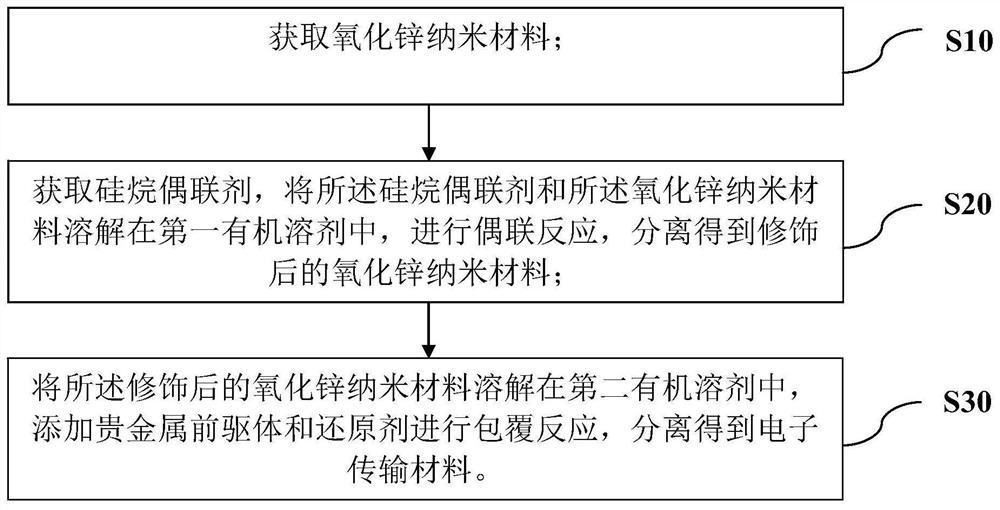
[0034] as attached figure 1 As shown, the second aspect of the embodiment of the present application provides a method for preparing an electron transport material, comprising the following steps:
[0035] S10. Obtain zinc oxide nanomaterials;
[0036] S20. Obtain a silane coupling agent, dissolve the silane coupling agent and the zinc oxide nanomaterial in the first organic solvent, perform a coupling reaction, and separate and obtain the modified zinc oxide nanomaterial;
[0037] S30. Dissolving the modified zinc oxide nanomaterial in a second organic solvent, adding a noble metal precursor and a reducing agent to carry out a coating reaction, and separating to obtain an electron transport material.
[0038] The preparation method of the electron transport material provided by the second aspect of the present application uses a silane coupling agent to modify the surface of the zinc oxide nanomaterial. The organic functional group in the silane coupling agent has binding pr...
Embodiment 1
[0105] An electron transport thin film, comprising the following preparation steps:
[0106] ① Add an appropriate amount of zinc chloride to 50mL of ethanol to form a solution with a concentration of 0.5M, stir and dissolve at 70°C. Add potassium hydroxide dissolved in 10mL ethanol lye (molar ratio, OH - : Zn 2+ =1.8:1, pH=12). Stirring was continued at 70 °C for 4 h to obtain a homogeneous solution. Subsequently, after the solution was cooled, it was precipitated with ethyl acetate, and after centrifugation, it was dissolved with a small amount of ethanol, and the steps of precipitation and dissolution were repeated three times, followed by drying to obtain ZnO nanoparticles.
[0107] ②Weigh an appropriate amount of ZnO into a flask, and add 50mL of absolute ethanol to it to form a solution with a concentration of 0.5M. Add 3-aminopropyltriethoxysilane (APTES) (molar ratio, ZnO:APTES=1:1) into the flask, stir and reflux at room temperature for 7 hours under an inert atmos...
Embodiment 2
[0111] An electron transport thin film, comprising the following preparation steps:
[0112] ① First, add an appropriate amount of zinc nitrate to 50mL of methanol to form a solution with a total concentration of 0.8M. Then stir and dissolve at 60°C, add sodium hydroxide dissolved in 10mL ethanol lye (molar ratio, OH - : Zn 2+ =1.8:1, pH=12). Stirring was continued at 60 °C for 4 h to obtain a homogeneous solution. Subsequently, after the solution is cooled, it is precipitated with heptane, and after centrifugation, it is dissolved with a small amount of methanol (repeat the operation and wash 3 times) to obtain ZnO nanoparticles.
[0113] ② Weigh an appropriate amount of ZnO into a flask, and add 50mL of absolute ethanol to it to form a solution with a concentration of 0.8M. Add aminopropyltrimethoxysilane (APS) (molar ratio, ZnO:APS=1:1.5) into the flask, stir and reflux at room temperature for 8h under an inert atmosphere. Subsequently, it was precipitated with heptane...
PUM
| Property | Measurement | Unit |
|---|---|---|
| thickness | aaaaa | aaaaa |
| particle diameter | aaaaa | aaaaa |
| particle diameter | aaaaa | aaaaa |
Abstract
Description
Claims
Application Information
 - R&D Engineer
- R&D Manager
- IP Professional
- Industry Leading Data Capabilities
- Powerful AI technology
- Patent DNA Extraction
Browse by: Latest US Patents, China's latest patents, Technical Efficacy Thesaurus, Application Domain, Technology Topic, Popular Technical Reports.
© 2024 PatSnap. All rights reserved.Legal|Privacy policy|Modern Slavery Act Transparency Statement|Sitemap|About US| Contact US: help@patsnap.com