Double-channel MOSFET semiconductor device

A dual-channel, semiconductor technology, used in semiconductor devices, electrical components, circuits, etc., to achieve the effects of reducing on-resistance, smoothing the concentration of electric fields, and increasing density

Pending Publication Date: 2022-04-22
SUZHOU SILIKRON SEMICON CO LTD
View PDF0 Cites 0 Cited by
  • Summary
  • Abstract
  • Description
  • Claims
  • Application Information

AI Technical Summary

Problems solved by technology

Prior art MOSFET devices such as figure 1 As shown, the prior art MOSFET on-resistance still has room for improvement

Method used


Image

  • Double-channel MOSFET semiconductor device
  • Double-channel MOSFET semiconductor device
  • Double-channel MOSFET semiconductor device

Examples


Embodiment 1

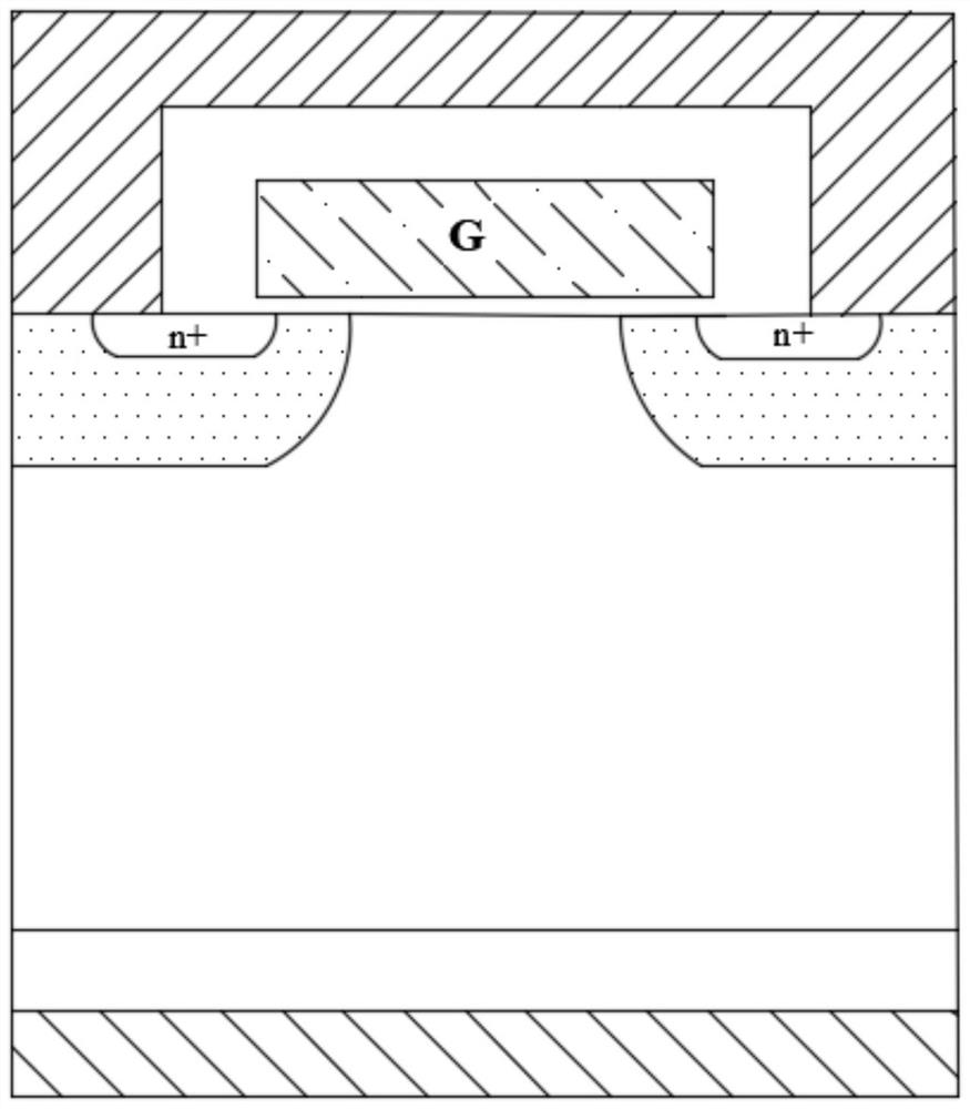
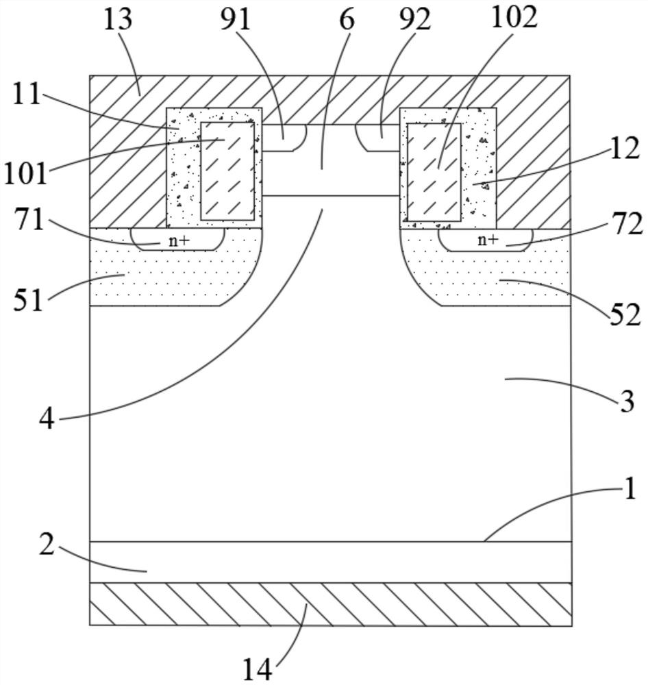
[0019] Embodiment 1: A kind of dual-channel MOSFET semiconductor device, comprising: the heavily doped N-type drain layer 2 located at the lower part of the silicon wafer 1 and the N-type doped epitaxial layer 3 located at the middle and upper part of the silicon wafer 1, the N-type The central region 8 of the doped epitaxial layer 3 has a raised portion 4 extending upward, and the upper part of the N-type doped epitaxial layer 3 and the two sides of the central region 8 respectively have a P-type left base region 51 and a P-type right base region. region 52, the upper part of the raised portion 4 has a P-type upper base region 6, and the upper parts of the P-type left base region 51 and the P-type right base region 52 respectively have a heavily doped N-type left source region 71 and The heavily doped N-type right source region 72, the upper part of the P-type upper base region 6 and the left and right sides are alternately provided with a heavily doped N-type upper left sourc...

Embodiment 2

[0024] Embodiment 2: A kind of dual-channel MOSFET semiconductor device, comprising: the heavily doped N-type drain layer 2 located at the lower part of the silicon wafer 1 and the N-type doped epitaxial layer 3 located at the middle and upper part of the silicon wafer 1, the N-type The central region 8 of the doped epitaxial layer 3 has a raised portion 4 extending upward, and the upper part of the N-type doped epitaxial layer 3 and the two sides of the central region 8 respectively have a P-type left base region 51 and a P-type right base region. region 52, the upper part of the raised portion 4 has a P-type upper base region 6, and the upper parts of the P-type left base region 51 and the P-type right base region 52 respectively have a heavily doped N-type left source region 71 and The heavily doped N-type right source region 72, the upper part of the P-type upper base region 6 and the left and right sides are alternately provided with a heavily doped N-type upper left sourc...


PUM


Abstract

The invention discloses a double-channel type MOSFET (Metal-Oxide-Semiconductor Field Effect Transistor) semiconductor device, which comprises a heavily doped N-type drain electrode layer positioned at the lower part of a silicon wafer and an N-type doped epitaxial layer positioned at the middle upper part of the silicon wafer, a left gate region and a right gate region which are respectively positioned at two sides of a convex part, the left gate region is located above the P-type left base region between the heavily doped N-type left source region and the central region, the right gate region is located above the P-type right base region between the heavily doped N-type right source region and the central region, and the right side and the lower part of the left gate region are electrically isolated from the P-type upper base region and the P-type left base region through a first insulating layer; and the left side and the lower part of the right gate region are electrically isolated from the P-type upper base region and the P-type right base region through a second insulating layer. According to the invention, the density of a current channel is effectively increased in a unit area, so that the on resistance of the device is effectively reduced, and the device also has a better voltage withstanding characteristic.

Description

technical field [0001] The invention relates to the technical field of MOSFET devices, in particular to a double-channel MOSFET semiconductor device. Background technique [0002] Trench power MOSFET is a new high-efficiency switching device developed after planar VDMOS. It is widely used in the field of power electronics because of its high input impedance, small driving current, fast switching speed, and good high-temperature characteristics. Prior art MOSFET devices such as figure 1 As shown, there is still room for improvement in the prior art MOSFET on-resistance. Contents of the invention [0003] The object of the present invention is to provide a kind of double-channel type MOSFET semiconductor device, this double-channel type MOSFET semiconductor device has not only effectively increased the density of the current channel in the unit area, the on-resistance of the device is effectively reduced, but also has Better withstand voltage characteristics. [0004] In ...

Claims


Application Information

Patent Timeline
Patent Type & Authority Applications(China)
IPC IPC(8): H01L29/78H01L29/423
CPCH01L29/7813H01L29/4236
Inventor 陈译陆佳顺杨洁雯
Owner SUZHOU SILIKRON SEMICON CO LTD
Why Eureka
Try Eureka