Flexible antimony selenide/perovskite laminated solar cell and preparation method thereof
A technology of solar cells and antimony selenide, which is applied in the field of solar cells, can solve the problems of limiting photoelectric conversion efficiency and narrow light absorption range, and achieve the effects of broadening the spectral absorption range, broadening the utilization range, and reducing thermal relaxation loss
- Summary
- Abstract
- Description
- Claims
- Application Information
AI Technical Summary
Problems solved by technology
Method used
Image
Examples
preparation example Construction
[0045] The present invention also provides a method for preparing the above-mentioned flexible antimony selenide / perovskite laminated solar cell, comprising: S1) depositing a back electrode on a substrate to obtain a composite back electrode substrate; S2) depositing a composite back electrode on the substrate; Evaporating an antimony selenide absorbing layer on the substrate of the back electrode to obtain a composite antimony selenide absorbing layer substrate; S3) depositing a buffer layer on the composite antimony selenide absorbing layer substrate to obtain a composite buffer layer substrate; S4) depositing a window layer on the substrate of the composite buffer layer to obtain the substrate of the composite window layer; S5) depositing an intermediate composite layer on the substrate of the composite window layer to obtain the substrate of the composite intermediate composite layer; S6) Prepare a hole transport layer on the substrate of the composite intermediate composit...
Embodiment 1
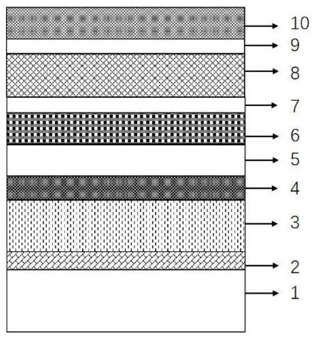
[0060] 1) Select a stainless steel foil (1) with a thickness of 0.3 mm, grind and polish it, and then use deionized water, absolute ethanol and acetone to ultrasonically clean it for 30 minutes, and then N 2 blow dry;
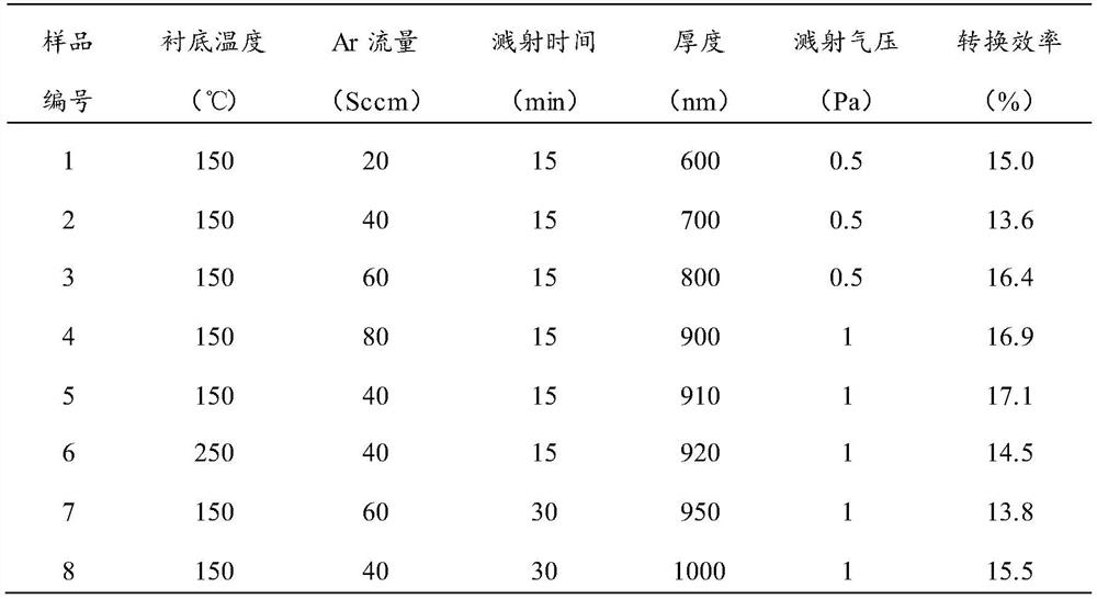
[0061] 2) Preparation of the metal back electrode (2): Mo was deposited on the stainless steel foil (1) by magnetron sputtering as Sb 2 Se 3 The back electrode of the battery, the parameters are as follows: sputtering power 120W, sputtering pressure 0.4~1.2Pa, sputtering time 15~30min, equipment vacuum degree 2.0×10 -4 Pa, target base distance 50mm, substrate temperature 50-250°C, Ar flow rate 20-80sccm, the prepared back electrode thickness is 600-1000nm (see Table 1 for details);
[0062] 3) Sb 2 Se 3 Preparation of the absorbing layer (3): when the degree of vacuum is less than 1*10 -4 Under Pa, a layer of Sb with a thickness of 300nm was evaporated at 500°C by vacuum evaporation at an evaporation rate of 0.8 angstroms per second. 2 Se 3 layer
[006...
Embodiment 2
[0074] 1) Select a stainless steel foil (1) with a thickness of 0.3 mm, grind and polish it, and then use deionized water, absolute ethanol and acetone to ultrasonically clean it for 30 minutes, and then N 2 blow dry;
[0075] 2) Preparation of the metal back electrode (2): Mo was deposited on the stainless steel foil (1) by magnetron sputtering as Sb 2 Se 3 The back electrode of the battery, the parameters are as follows: sputtering power 120W, sputtering pressure 1Pa, sputtering time 15min, equipment vacuum degree 2.0×10 - 4 Pa, target base distance 50mm, substrate temperature 150°C, Ar flow rate 40sccm, the prepared back electrode thickness is 910nm;
[0076] 3) Sb 2 Se 3 Preparation of the absorbing layer (3): when the degree of vacuum is less than 1*10 -4 Under Pa, a layer of Sb with a thickness of 300nm was evaporated at 500°C by vacuum evaporation at an evaporation rate of 0.8 angstroms per second. 2 Se 3 layer.
[0077] 4) The preparation of buffer layer (4): ...
PUM
| Property | Measurement | Unit |
|---|---|---|
| thickness | aaaaa | aaaaa |
| thickness | aaaaa | aaaaa |
| thickness | aaaaa | aaaaa |
Abstract
Description
Claims
Application Information
 - Generate Ideas
- Intellectual Property
- Life Sciences
- Materials
- Tech Scout
- Unparalleled Data Quality
- Higher Quality Content
- 60% Fewer Hallucinations
Browse by: Latest US Patents, China's latest patents, Technical Efficacy Thesaurus, Application Domain, Technology Topic, Popular Technical Reports.
© 2025 PatSnap. All rights reserved.Legal|Privacy policy|Modern Slavery Act Transparency Statement|Sitemap|About US| Contact US: help@patsnap.com


